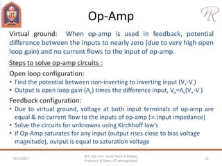
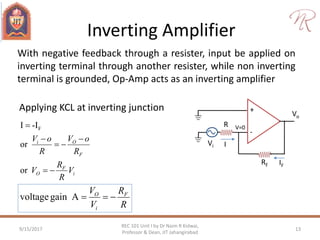
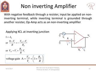
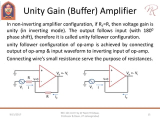
Operational Amplifiers
Operational Amplifiers : Introduction and Block diagram of Op Amp, Ideal &
Practical characteristics of Op Amp, Differential amplifier circuits, Practical
OpAmp Circuits (Inverting Amplifier, Non inverting Amplifier, Unity Gain
Amplifier, Summing Amplifier, Integrator, Differentiator). OPAMP
Parameters: Input offset voltage, Output offset voltage, Input biased
current, Input offset current Differential and Common-Mode Operation
9/15/2017 1
REC 101 Unit I by Dr Naim R Kidwai,
Professor & Dean, JIT Jahangirabad
Introduction and Block diagram of Op-Amp
9/15/2017 2
REC 101 Unit I by Dr Naim R Kidwai,
Professor & Dean, JIT Jahangirabad
• Op-Amp or operational amplifiers, is a very high gain differential
amplifier with high input impedance and low output impedance.
• Op-Amp find common application in mathematical operations like
addition, subtraction, integration etc. thus term operational is given
• Nowadays op-amps are IC based (Integrated circuit) that require
relatively low power, reliable and inexpensive.
• Op-Amp’s originated around 1947
+
-
+VCC
-VEE
Non Inverting
input
Inverting
input
OutputAV
Op-Amp
741
1 2 3 4
8 7 6 5
OffsetNull
Inverting
NonInverting
-VEE
VCC
Output
OffsetNull
Open
+
-
Non Inverting
input
Inverting
input
OutputAV
Introduction and Block diagram of Op-Amp
9/15/2017 3
REC 101 Unit I by Dr Naim R Kidwai,
Professor & Dean, JIT Jahangirabad
• A typical op-amp is made up of three stages;
• differential amplifier stage
• voltage amplifier
• push-pull amplifier stage
• Input stage of op-amp is differential amplifier. It provides
amplification of the difference voltage between the two inputs.
• The second stage is a class A amplifier that provides additional
gain. Some op-amps may have more voltage amplifier stages
• A push-pull class B amplifier is typically used for the output stage.
Differential
amplifier Input
stage
Voltage
amplifier gain
stage
Push-pull
amplifier
output stage
+
-
Vd
output
Op Amp Modes of operation
9/15/2017 4
REC 101 Unit I by Dr Naim R Kidwai,
Professor & Dean, JIT Jahangirabad
Single Differential mode
+
-
AV
Vi
Vo = AV Vi
+
-
AV
Vi
Vo = -AV Vi
double Differential mode
+
-
AV
V1
Vo = AV(V1–V2)
V2
+
-
AVVi
Vo = AVVi
Differential Mode: In Differential mode, output of op-amp
input;aldifferentigain,voltagealdifferentiwhere  

VVVVA
VAV
ddv
dvo
Op-Amp Parameters
Open loop Voltage gain (Av): The open-
loop gain of an Op-Amp is the gain obtained
with respect to differential input when op-
amp is used in open loop (no feedback)
Output offset voltage VOO: In practical op-
amp, a small dc voltage called output offset
voltage VOO, appears at the output when no
differential input voltage is applied.
Input offset voltage VOS: is the differential
dc voltage required between the inputs to
force the output to zero volts. Typical
values of input offset voltage are upto 2 mV.
Ideally VOS is 0 V.
9/15/2017 5
REC 101 Unit I by Dr Naim R Kidwai,
Professor & Dean, JIT Jahangirabad
+
-
AVVd
Vo = AVVd
+
-
AVVOS
VO =0
+
-
AV
VOO
Op-Amp Parameters
Input biased current (IBias): is the average of
currents at both inputs of Op-amp (required to
operate properly amplifier first stage).
Input offset current (IOS): Ideally, the two
input bias currents are equal, but practically is
not. IOS is the absolute difference of the input
bias currents. (with magnitudes at least ten
times less than the bias current.
Slew Rate: is maximum rate of change of the
output voltage in response to a step input.
Slew rate depends upon the high-frequency
response of the amplifier stages of op-amp.
Slew rate =maximum rate at which Op-Amp
output can change (V/s)
9/15/2017 6
REC 101 Unit I by Dr Naim R Kidwai,
Professor & Dean, JIT Jahangirabad
+
-
AV
VO
V1
V2
I2
I1
2
21 II
IBias


21 IIIOS 
+
-
Vo
Vi
t
Vi
t
V0
Op-Amp Parameters
Input biased current (IBias): is the average of currents at both inputs of
Op-amp (required to operate properly amplifier first stage).
Input offset current (IOS): Ideally, the two input bias currents are
equal, but practically is not. IOS is the absolute difference of the input
bias currents. (with magnitudes at least ten times less than IBias)
9/15/2017 7
REC 101 Unit I by Dr Naim R Kidwai,
Professor & Dean, JIT Jahangirabad
+
-
AV
VO
V1
V2
I2
I1
2
21 II
IBias

 21 IIIOS 
+
-
Vo
Vi
t
Vi
Slew Rate: is maximum rate of change of the output voltage in
response to a step input expressed in V/s. Slew rate depends upon
the high-frequency response of the amplifier stages of op-amp
t
V0 t
V t
V


rateSlew
Op Amp Modes of operation
9/15/2017 8
REC 101 Unit I by Dr Naim R Kidwai,
Professor & Dean, JIT Jahangirabad
+
-
AV
Vi
Vo = 0
Vi
Common mode operation: In common mode common input is
applied on both inputs of op-amp. The difference applied is zero so
the output is zero. This action is called common mode rejection
Common mode rejection ratio (CMRR): Practical op-amps provide
small common mode gain with very large differential mode gain.
CMRR is defined as
It means that unwanted signal appearing on both
inputs will be rejected and will not distort output








cm
OL
A
A
dBCMRR
CMRR
log20)(
)(Againvoltagemodecommon
)(AgainvoltagealdifferentiloopOpen
cm
OL
Ideal & Practical characteristics of Op Amp
9/15/2017 9
REC 101 Unit I by Dr Naim R Kidwai,
Professor & Dean, JIT Jahangirabad
ideal practical
Differential Voltage gain  106
bandwidth  MHz
Input impedance  M
output impedance 0 100’s 
Slew rate  0.5 V/s
CMRR  90 dB
Input offset voltage 0 1 mV
Ideal and practical characteristics of op-amp is given in table below
Differential amplifier circuits
9/15/2017 10
REC 101 Unit I by Dr Naim R Kidwai,
Professor & Dean, JIT Jahangirabad
The differential amplifier circuit is an extremely popular circuit used.
It has two separate inputs and two separate outputs which are
related to difference of inputs.
Differential amplifier works in differential & common mode
• If an input signal is applied to either input with the other input connected to
ground, the operation is referred to as “single-ended differential mode.”
• If two different input signals are applied, the operation is referred to as “double-
ended differential mode.”
• If the same input is applied to both inputs, the operation is called common-mode
Main feature of differential amplifier is very large gain for differential
input as compared to the very small gain for common inputs. The
ratio of this difference gain to the common gain is called common-
mode rejection.
Differential amplifier circuits
9/15/2017 11
REC 101 Unit I by Dr Naim R Kidwai,
Professor & Dean, JIT Jahangirabad
Q1 Q2
RE
RC
RC
VCC
-VEE
VO2VO1
Vi1 Vi2
Vo1
Vi2 Vo2
Vi1
Differential amplifier circuit using BJT
Differential amplifier Symbolic notation
Op-Amp
9/15/2017 12
REC 101 Unit I by Dr Naim R Kidwai,
Professor & Dean, JIT Jahangirabad
Virtual ground: When op-amp is used in feedback, potential
difference between the inputs to nearly zero (due to very high open
loop gain) and no current flows to the input of op-amp.
Steps to solve op-amp circuits :
Open loop configuration:
• Find the potential between non-inverting to inverting input (V+-V-)
• Output is open loop gain (Av) times the difference input, Vo=Av(V+-V-)
Feedback configuration:
• Due to virtual ground, voltage at both input terminals of op-amp are
equal & no current flow to the inputs of op-amp ( input impedance)
• Solve the circuits for unknowns using Kirchhoff law’s
• If Op-Amp saturates for any input (output rises close to bias voltage
magnitude), output is equal to saturation voltage
Inverting Amplifier
Applying KCL at inverting junction
9/15/2017 13
REC 101 Unit I by Dr Naim R Kidwai,
Professor & Dean, JIT Jahangirabad
+
-
Vo
RF
Vi
R V=0
I
IF
i
F
O
F
Oi
V
R
R
V
R
oV
R
oV





or
or
-II F
R
R
V
V F
i
O
Againvoltage
With negative feedback through a resister, input be applied on
inverting terminal through another resister, while non inverting
terminal is grounded, Op-Amp acts as an inverting amplifier
Non inverting Amplifier
9/15/2017 14
REC 101 Unit I by Dr Naim R Kidwai,
Professor & Dean, JIT Jahangirabad
Applying KCL at inverting junction
+
-
Vo
RF
Vi
R Vi
I
IF
i
F
iO
F
iOi
V
R
R
VV
R
VV
R
V





or
0
or
-II F







R
R
V
V F
i
O
1Againvoltage
With negative feedback through a resister, input be applied on non-
inverting terminal, while inverting terminal is grounded through
another resister, Op-Amp acts as an non-inverting amplifier
Unity Gain (Buffer) Amplifier
9/15/2017 15
REC 101 Unit I by Dr Naim R Kidwai,
Professor & Dean, JIT Jahangirabad
+
-
Vo =- Vi
R
Vi
R V=0
I
IF
In non-inverting amplifier configuration, if RF=R, then voltage gain is
unity (in inverting mode). The output follows input (with 1800
phase shift), therefore it is called unity follower configuration.
unity follower configuration of op-amp is achieved by connecting
output of op-amp & input waveform to inverting input of op-amp.
Connecting wire’s small resistance serve the purpose of resistances.
+
-
Vo =- Vi
Vi
V=0
I
IF
Summing Amplifier
A popular application of an op-amp is as a summing amplifier.
Various input voltages can be summed (each multiplied by a
different weight) as shown in below circuit
9/15/2017 16
REC 101 Unit I by Dr Naim R Kidwai,
Professor & Dean, JIT Jahangirabad
+
-
Vo
RF
R2 V=0
I2
IF
V2
R1
I1
V1
R3
I3
V3
Applying KCL at inverting junction
F
O
R
oV
R
oV
R
oV
R
oV 







3
3
2
2
1
1
F321
or
-IIII
 321321
3
3
2
2
1
1
thenIf VVVVRRRR
V
R
R
V
R
R
V
R
R
V
OF
FFF
O








Integrator
Op-amp can be used as a integrator with feedback capacitor
connected at inverting terminal and applying input through a
resistor at inverting terminal
9/15/2017 17
REC 101 Unit I by Dr Naim R Kidwai,
Professor & Dean, JIT Jahangirabad
Applying KCL at inverting junction
 0
0
or
-II F



O
i
V
dt
d
C
R
V
+
-
Vo
C
Vi
R V=0
I
IF

t
iO dV
RC
V
0
1

Differentiator
9/15/2017 18
REC 101 Unit I by Dr Naim R Kidwai,
Professor & Dean, JIT Jahangirabad
Op-amp can be used as a differentiator by with applying input
through a capacitor inverting terminal and negative feedback
Applying KCL at inverting junction
 
R
V
V
dt
d
C i
0
0or
-II
0
F



+
-
Vo
Vi R
V=0
I
IF
C
iO V
dt
d
RCV 

Rec101 unit iii operational amplifier

  • 1.
    Operational Amplifiers Operational Amplifiers: Introduction and Block diagram of Op Amp, Ideal & Practical characteristics of Op Amp, Differential amplifier circuits, Practical OpAmp Circuits (Inverting Amplifier, Non inverting Amplifier, Unity Gain Amplifier, Summing Amplifier, Integrator, Differentiator). OPAMP Parameters: Input offset voltage, Output offset voltage, Input biased current, Input offset current Differential and Common-Mode Operation 9/15/2017 1 REC 101 Unit I by Dr Naim R Kidwai, Professor & Dean, JIT Jahangirabad
  • 2.
    Introduction and Blockdiagram of Op-Amp 9/15/2017 2 REC 101 Unit I by Dr Naim R Kidwai, Professor & Dean, JIT Jahangirabad • Op-Amp or operational amplifiers, is a very high gain differential amplifier with high input impedance and low output impedance. • Op-Amp find common application in mathematical operations like addition, subtraction, integration etc. thus term operational is given • Nowadays op-amps are IC based (Integrated circuit) that require relatively low power, reliable and inexpensive. • Op-Amp’s originated around 1947 + - +VCC -VEE Non Inverting input Inverting input OutputAV Op-Amp 741 1 2 3 4 8 7 6 5 OffsetNull Inverting NonInverting -VEE VCC Output OffsetNull Open + - Non Inverting input Inverting input OutputAV
  • 3.
    Introduction and Blockdiagram of Op-Amp 9/15/2017 3 REC 101 Unit I by Dr Naim R Kidwai, Professor & Dean, JIT Jahangirabad • A typical op-amp is made up of three stages; • differential amplifier stage • voltage amplifier • push-pull amplifier stage • Input stage of op-amp is differential amplifier. It provides amplification of the difference voltage between the two inputs. • The second stage is a class A amplifier that provides additional gain. Some op-amps may have more voltage amplifier stages • A push-pull class B amplifier is typically used for the output stage. Differential amplifier Input stage Voltage amplifier gain stage Push-pull amplifier output stage + - Vd output
  • 4.
    Op Amp Modesof operation 9/15/2017 4 REC 101 Unit I by Dr Naim R Kidwai, Professor & Dean, JIT Jahangirabad Single Differential mode + - AV Vi Vo = AV Vi + - AV Vi Vo = -AV Vi double Differential mode + - AV V1 Vo = AV(V1–V2) V2 + - AVVi Vo = AVVi Differential Mode: In Differential mode, output of op-amp input;aldifferentigain,voltagealdifferentiwhere    VVVVA VAV ddv dvo
  • 5.
    Op-Amp Parameters Open loopVoltage gain (Av): The open- loop gain of an Op-Amp is the gain obtained with respect to differential input when op- amp is used in open loop (no feedback) Output offset voltage VOO: In practical op- amp, a small dc voltage called output offset voltage VOO, appears at the output when no differential input voltage is applied. Input offset voltage VOS: is the differential dc voltage required between the inputs to force the output to zero volts. Typical values of input offset voltage are upto 2 mV. Ideally VOS is 0 V. 9/15/2017 5 REC 101 Unit I by Dr Naim R Kidwai, Professor & Dean, JIT Jahangirabad + - AVVd Vo = AVVd + - AVVOS VO =0 + - AV VOO
  • 6.
    Op-Amp Parameters Input biasedcurrent (IBias): is the average of currents at both inputs of Op-amp (required to operate properly amplifier first stage). Input offset current (IOS): Ideally, the two input bias currents are equal, but practically is not. IOS is the absolute difference of the input bias currents. (with magnitudes at least ten times less than the bias current. Slew Rate: is maximum rate of change of the output voltage in response to a step input. Slew rate depends upon the high-frequency response of the amplifier stages of op-amp. Slew rate =maximum rate at which Op-Amp output can change (V/s) 9/15/2017 6 REC 101 Unit I by Dr Naim R Kidwai, Professor & Dean, JIT Jahangirabad + - AV VO V1 V2 I2 I1 2 21 II IBias   21 IIIOS  + - Vo Vi t Vi t V0
  • 7.
    Op-Amp Parameters Input biasedcurrent (IBias): is the average of currents at both inputs of Op-amp (required to operate properly amplifier first stage). Input offset current (IOS): Ideally, the two input bias currents are equal, but practically is not. IOS is the absolute difference of the input bias currents. (with magnitudes at least ten times less than IBias) 9/15/2017 7 REC 101 Unit I by Dr Naim R Kidwai, Professor & Dean, JIT Jahangirabad + - AV VO V1 V2 I2 I1 2 21 II IBias   21 IIIOS  + - Vo Vi t Vi Slew Rate: is maximum rate of change of the output voltage in response to a step input expressed in V/s. Slew rate depends upon the high-frequency response of the amplifier stages of op-amp t V0 t V t V   rateSlew
  • 8.
    Op Amp Modesof operation 9/15/2017 8 REC 101 Unit I by Dr Naim R Kidwai, Professor & Dean, JIT Jahangirabad + - AV Vi Vo = 0 Vi Common mode operation: In common mode common input is applied on both inputs of op-amp. The difference applied is zero so the output is zero. This action is called common mode rejection Common mode rejection ratio (CMRR): Practical op-amps provide small common mode gain with very large differential mode gain. CMRR is defined as It means that unwanted signal appearing on both inputs will be rejected and will not distort output         cm OL A A dBCMRR CMRR log20)( )(Againvoltagemodecommon )(AgainvoltagealdifferentiloopOpen cm OL
  • 9.
    Ideal & Practicalcharacteristics of Op Amp 9/15/2017 9 REC 101 Unit I by Dr Naim R Kidwai, Professor & Dean, JIT Jahangirabad ideal practical Differential Voltage gain  106 bandwidth  MHz Input impedance  M output impedance 0 100’s  Slew rate  0.5 V/s CMRR  90 dB Input offset voltage 0 1 mV Ideal and practical characteristics of op-amp is given in table below
  • 10.
    Differential amplifier circuits 9/15/201710 REC 101 Unit I by Dr Naim R Kidwai, Professor & Dean, JIT Jahangirabad The differential amplifier circuit is an extremely popular circuit used. It has two separate inputs and two separate outputs which are related to difference of inputs. Differential amplifier works in differential & common mode • If an input signal is applied to either input with the other input connected to ground, the operation is referred to as “single-ended differential mode.” • If two different input signals are applied, the operation is referred to as “double- ended differential mode.” • If the same input is applied to both inputs, the operation is called common-mode Main feature of differential amplifier is very large gain for differential input as compared to the very small gain for common inputs. The ratio of this difference gain to the common gain is called common- mode rejection.
  • 11.
    Differential amplifier circuits 9/15/201711 REC 101 Unit I by Dr Naim R Kidwai, Professor & Dean, JIT Jahangirabad Q1 Q2 RE RC RC VCC -VEE VO2VO1 Vi1 Vi2 Vo1 Vi2 Vo2 Vi1 Differential amplifier circuit using BJT Differential amplifier Symbolic notation
  • 12.
    Op-Amp 9/15/2017 12 REC 101Unit I by Dr Naim R Kidwai, Professor & Dean, JIT Jahangirabad Virtual ground: When op-amp is used in feedback, potential difference between the inputs to nearly zero (due to very high open loop gain) and no current flows to the input of op-amp. Steps to solve op-amp circuits : Open loop configuration: • Find the potential between non-inverting to inverting input (V+-V-) • Output is open loop gain (Av) times the difference input, Vo=Av(V+-V-) Feedback configuration: • Due to virtual ground, voltage at both input terminals of op-amp are equal & no current flow to the inputs of op-amp ( input impedance) • Solve the circuits for unknowns using Kirchhoff law’s • If Op-Amp saturates for any input (output rises close to bias voltage magnitude), output is equal to saturation voltage
  • 13.
    Inverting Amplifier Applying KCLat inverting junction 9/15/2017 13 REC 101 Unit I by Dr Naim R Kidwai, Professor & Dean, JIT Jahangirabad + - Vo RF Vi R V=0 I IF i F O F Oi V R R V R oV R oV      or or -II F R R V V F i O Againvoltage With negative feedback through a resister, input be applied on inverting terminal through another resister, while non inverting terminal is grounded, Op-Amp acts as an inverting amplifier
  • 14.
    Non inverting Amplifier 9/15/201714 REC 101 Unit I by Dr Naim R Kidwai, Professor & Dean, JIT Jahangirabad Applying KCL at inverting junction + - Vo RF Vi R Vi I IF i F iO F iOi V R R VV R VV R V      or 0 or -II F        R R V V F i O 1Againvoltage With negative feedback through a resister, input be applied on non- inverting terminal, while inverting terminal is grounded through another resister, Op-Amp acts as an non-inverting amplifier
  • 15.
    Unity Gain (Buffer)Amplifier 9/15/2017 15 REC 101 Unit I by Dr Naim R Kidwai, Professor & Dean, JIT Jahangirabad + - Vo =- Vi R Vi R V=0 I IF In non-inverting amplifier configuration, if RF=R, then voltage gain is unity (in inverting mode). The output follows input (with 1800 phase shift), therefore it is called unity follower configuration. unity follower configuration of op-amp is achieved by connecting output of op-amp & input waveform to inverting input of op-amp. Connecting wire’s small resistance serve the purpose of resistances. + - Vo =- Vi Vi V=0 I IF
  • 16.
    Summing Amplifier A popularapplication of an op-amp is as a summing amplifier. Various input voltages can be summed (each multiplied by a different weight) as shown in below circuit 9/15/2017 16 REC 101 Unit I by Dr Naim R Kidwai, Professor & Dean, JIT Jahangirabad + - Vo RF R2 V=0 I2 IF V2 R1 I1 V1 R3 I3 V3 Applying KCL at inverting junction F O R oV R oV R oV R oV         3 3 2 2 1 1 F321 or -IIII  321321 3 3 2 2 1 1 thenIf VVVVRRRR V R R V R R V R R V OF FFF O        
  • 17.
    Integrator Op-amp can beused as a integrator with feedback capacitor connected at inverting terminal and applying input through a resistor at inverting terminal 9/15/2017 17 REC 101 Unit I by Dr Naim R Kidwai, Professor & Dean, JIT Jahangirabad Applying KCL at inverting junction  0 0 or -II F    O i V dt d C R V + - Vo C Vi R V=0 I IF  t iO dV RC V 0 1 
  • 18.
    Differentiator 9/15/2017 18 REC 101Unit I by Dr Naim R Kidwai, Professor & Dean, JIT Jahangirabad Op-amp can be used as a differentiator by with applying input through a capacitor inverting terminal and negative feedback Applying KCL at inverting junction   R V V dt d C i 0 0or -II 0 F    + - Vo Vi R V=0 I IF C iO V dt d RCV 