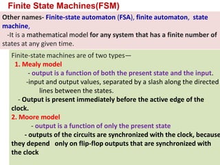
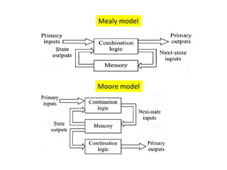
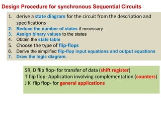
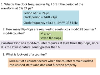
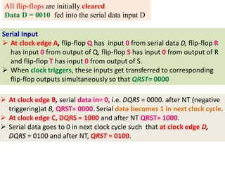
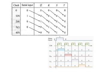
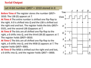
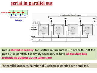
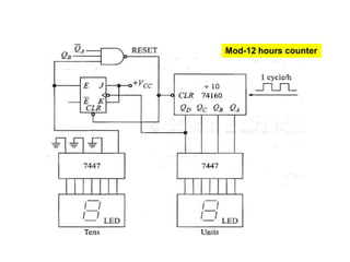
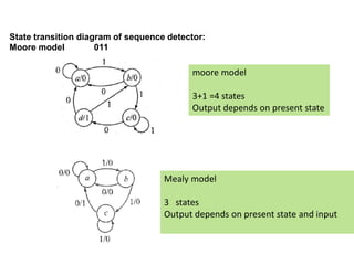
Dr.C.Helen Sulochana
Prof/ECE
SXCCE
SYNCHRONOUS SEQUENTIAL CIRCUITS
Latches, Flip flops – SR, JK, T, D, Master/Slave FF,
Triggering of FF, Analysis and design of clocked
sequential circuits – Design - Moore/Mealy models,
state minimization, state assignment, lock - out
condition circuit implementation - Counters, Ripple
Counters, Ring Counters, Shift registers, Universal
Shift Register. Model Development: Designing of
rolling display/real time clock
SEQUENTIAL CIRCUITS
Block diagram of sequential circuit
 sequential circuits consists of combinational circuit connected to a
storage elements in the feedback path
 State of the sequential circuit at any given time is the binary
information stored in the storage element at that time
 next state of the storage elements is a function of external inputs and
the present state of storage elements.
A sequential circuit is specified by a time sequence of
inputs, outputs, and internal states
output depends upon present as well as past input
Sl.No combinational circuit Sequential Circuit
1 output depends only upon present
input.
output depends upon present as
well as past input.
2 Speed is fast Speed is slow
3 No feedback between input and
output
There exists a feedback path
between input and output
4 Used for arithmetic as well as
boolean operations.
used for storing data
5 Elementary building blocks: Logic
gates
Elementary building blocks: Flip-
flops
6 No storage element, don’t have
clock, they don’t require triggering
Used as storage element. Clock
dependent, they need triggering
7 Used for arithmetic as well as
boolean operations.
Used for storing
Difference between sequential circuit & combinational circuit
1. synchronous sequential circuit
2. Asynchronous sequential circuit
Types of sequential circuit
1. Synchronous sequential circuit
Output of the circuit depends upon its input signals in
synchronization with the control signal (clock pulse)
The behavior of the circuit depends upon the input signals at
any instant of time and the order in which the inputs change
The storage elements commonly used in asynchronous
sequential circuits are time-delay devices or latches.
2. Asynchronous sequential circuit
Synchronous clocked sequential circuit
Latches
A Latch is a special type of logical circuit which has two stable- low(0)
and high(1)
Constructed with two cross-coupled NOR gates or two cross-coupled
NAND gates
SR Latch
Has two inputs S (set) and R(reset)
S input sets the output to logic1, R input reset the output to logic 0
two outputs Q and its complement 𝐐.
Logic diagram(NOR)
 When S =1, R=0, output of NOR gate 2 is low. Output of NOR gate 1 is 1(Q=1).
Therefore S= 1 , set the flip flop
 When S =0 ,R=1, output of NOR gate 1 is low. Output of NOR gate 2 is 0(Q=0).
Therefore R= 1 , reset the flip flop
Characteristic
table(function table or
truth table)
 When S =0 , R=0 and Q(previous state)= 0, both inputs to NOR
gate 2 are low, and its output Q‘= 1 and next state of Q = 0 (previous state)
When S =0 , R=0 and Q(previous state)= 1, Q’=0, both inputs to NOR
gate 1 are low, and its output Q‘= 0 and next state of Q = 1.
 When S =1 , R=1, both Q‘= 0 and Q = 0 , It is not possible because Q’ is
complement of Q
Logic symbol for SR latch
Logic diagram of SR Latch
using NAND gate
Same truth table as NOR
 storage elements (memory) used in clocked sequential circuits
 bistable electronic circuit that has two stable state , 0 and 1
Flip flop
Types of flip flops
1. SR (set, reset) Flip flop
2. JK Flip flop
3. D Flip flop
4. T Flip flop
1.SR flip flop
Logic diagram
using NOR gate
Function table Characteristic equation
Logic diagram
using NAND gate
Two inputs- S, R
Output –Q
Q’ is complement of Q
Expanded table
Logic symbol
Excitation table :
reverse of the truth table
By knowing the present and next state , find the inputs
Excitation table of SR flip flop
Note-for theory refer the material
2. D(delay) Flip flop (Transparent Latch)
-Application- used in Register and memory devices
Limitation of SR flip flop
S,R inputs can not be at logic 1 simultaneously
D flip flop overcome this limitation.
 S and R inputs are connected through an inverter
The input D is directly connected to S. It is inverted and connected to R
 output Q is always same as the input D, therefore called as data or D
flip flop
D flip flop from SR flip flop Logic symbol
If D = 1, the Q(t+1) output is 1, the circuit in the set state.
If D = 0, output Q goes to 0, the circuit in the reset state.
Data input D is transferred to the Q output when the clk input is
activated. Therefore called as transparent Flip flop.
One input- D
Output – Q
Logic diagram
using NOR gate
Logic diagram
using NAND gate
clk clk
Characteristic Equations
Excitation table
Truth table Expanded table
3. JK flip-flop
 S,R inputs can not be at logic 1 simultaneously in SR Flip flop
 This is over come in JK flip flop by connecting Q and Q’ outputs with
S and R inputs through AND gate
 When J=1 and K=1 , then the output Q will change state(toggle) as
long as clock is enabled.
J K flip flop from SR flip flop
Logic symbol
 When J=1, K=0, next clock edge sets the output Q=1, J input sets the
flip-flop to 1,
 When J=0, K=1, next state output Q=0, K input resets it to 0,
 when both inputs are high, the output is complemented
Two inputs- S, R
Output – Q
Logic diagram
using NOR gate
Logic diagram
using NAND gate
Expanded table
Characteristic Equation
Excitation table
Truth table
The T (toggle) flip-flop is a complementing flip-flop
obtained from a JK flip-flop when inputs J and K are tied together
4. T(Toggle) Flip flop
T flip flop from J K flip flop Logic symbol
Logic diagram using NOR gate
Logic diagram using NAND gate
Expanded table
Characteristic Equation
Excitation table
Truth table
Sl.No Flipflops Latches
1. edge-triggered devices Transparent or level triggered flip
flops
2 Change output only at
the transition of clock
input
Output Changes based on the input
only at the transition of enable input
2. storing binary(one bit)
information
useful for storing binary
information
3. storage elements
in synchronous
sequential circuits
Storage element in
asynchronous sequential
circuits,
Difference between laches and flip flops
Triggering the flip-flop
flip-flop is switched by a change in the control input. This momentary
change is called a trigger, and the transition it causes is said to trigger
the flip-flop.
Types of triggering
1. Level triggering
2. Edge triggering
2. Edge triggering
Edge triggering is a type of triggering that allows the output to
change depends on the input at the positive edge(clock pulse is
changing from 0(low) to high) or the negative edge edge(clock pulse
is changing from high to 0-low) of the clock signal.
1. Level triggering
level triggering is a type of triggering that allows the output to
change depends on the input when the clock pulse is on a particular
level (high or low).
edge triggering
level triggering
Direct Inputs to flip flop
Asynchronous(direct) inputs that are used to force the flip-flop to
a particular state independently of the clock
Input that sets the flip-flop to 1 is called preset or direct set .
The input that clears the flip-flop to 0 is called clear or direct reset
PR- preset CLR - clear
bubble along the input indicates that the reset is active at the logic-0
level.
1. Preset
2. clear
Master slave flip flops
 The master slave flip flop is constructed with two JK latches and an
inverter
 The first latch is called the master and the second as slave
For J-K flip-flop, if J=K=1, then output Q will toggle as long as clock
remains active which makes the output unstable. This is called as race
around condition
race around condition can be eliminated by
1.Edge triggering
2. Master- slave flpi flop
When the clock is 1, slave latch is disabled. The master latch is
enabled, and its output Q depends on the J and K input
When the clock is 0, the output of the inverter is 1. The slave latch is
enabled, and its output Q is equal to the master output Y
JK MASTER-SLAVE. FLIP-FLOPS
Master latch is set according to J and K while the clock is high;
contents of the master are then shifted into the slave (Q changes
state) when the clock goes low. This is referred to as pulse-
triggered
master
slave
Analysis and design of clocked sequential circuits
behavior of a clocked sequential circuit is determined from the
inputs, the outputs, and the state of its flip-flops.
analysis of a sequential circuit consists of
obtaining a table or a diagram for the time sequence of
inputs, outputs, and internal states
Example of sequential circuit
Input –x
Output –y
Flip flops – A, B
Example 1
Obtain the state table, state diagram, state equation for the following
circuit
SB =xA’
RB = x’A
SA =x’B
RA = xB’
The time sequence of inputs, outputs, and flip-flop states can be
represented in a state table
State Table(transition table )
 sequential circuit with m flipflops and n inputs needs 2m+n rows in
the state table.
 The next-state section has m columns, one for each flip-flop.
 The binary values for the next state are derived directly from the
state equations.
 The output section has as many columns as the output variables. Its
binary value is derived from the circuit
SB =xA’
RB = x’A
SA =x’B
RA = xB’
State Table
State Table in another form
Present state
A B
Input
x
Next state
A B
Flip flop input
SA, RA SB, RB
Output
y
0 0 0 0 0 0 0 0 0 0
0 0 1 0 1 0 1 1 0 0
0 1 0 1 1 1 0 0 0 0
0 1 1 0 1 0 0 1 0 0
1 0 0 1 0 0 0 0 1 0
1 0 1 0 0 0 1 0 0 1
1 1 0 1 0 1 0 0 1 0
1 1 1 1 1 0 0 0 0 0
State Diagram
Graphical representation of state table
 state is represented by a circle
 transitions between states are indicated by directed lines connecting
the circles
state of the flip-flops
input during the present state
output during the present
state
the directed line from state 00 to 01 is labeled 1/0, meaning that when the sequential
circuit is in the present state 00 and the input is 1, the output is 0. after the next clock
cycle,
State equation for A
A(t+1)= x’B +x’A+AB
State equation for B
B(t+1)=xA’ +xB+A’B
State equation from the state table Next state of A and B are marked in the K
map as a function of their present state and
input (minterms) to get the state equations
State Equations(application equation)
-Describe the behavior of a clocked sequential circuit
-specifies the next state as a function of the present state and inputs
Present
state
A B
Input
x
Next
state
A B
Flip flop input
SA, RA SB, RB
Output
y
0 0 0 0 0 0 0 0 0 0
0 0 1 0 1 0 1 1 0 0
0 1 0 1 1 1 0 0 0 0
0 1 1 0 1 0 0 1 0 0
1 0 0 1 0 0 0 0 1 0
1 0 1 0 0 0 1 0 0 1
1 1 0 1 0 1 0 0 1 0
1 1 1 1 1 0 0 0 0 0
Example 2
Draw the logic diagram for the following Boolean expression. Obtain the state table,
state diagram, state equation
logic diagram
State diagram of the circuit
input
State equation of flip-flop A
State equations for the flip-flops
State equation of flip-flop B
STATE REDUCTION AND ASSIGNMENT
To simplify the design of sequential circuit by reducing
the number of gates and flip-flops
State Reduction
reduction in the number of flip-flops in a sequential circuit is state-
reduction
m flip-flops produce 2m states
reduction in the number of states may (or may not) result in
a reduction in the number of flip-flops
Reduce the sequential circuit with the following State diagram
Example
Two states are equivalent if, they give same output and same next state or
an equivalent state, for each the set of inputs.
Form state table
 e and g has same next state
and output for same input
 Replace g by e
reduced table consists of only five states
satisfies the original input–output specifications
and will produce the required output sequence for any given input
sequence
Reduced state diagram
 f and d has same next state
and output for same input
 Replace g by e
Assigning unique coded binary values to the states
State Assignment
1. Binary - For m states, the codes must contain n bits, where 2n ≤ m
For five states, 3 bit code is used
23 = 8 ≤ 5(m), First five binary numbers are assigned to five states
Remaining 3 unused states are treated as don’t-care conditions during
the design to simplify the circuit
Other assignment method
2. Gray code -only one bit changes from one number to the next
3. one-hot assignment -At any given time, only one bit is equal to 1
while all others are kept at 0.
faster than binary encoding
Finite State Machines(FSM)
Other names- Finite-state automaton (FSA), finite automaton, state
machine,
-It is a mathematical model for any system that has a finite number of
states at any given time.
Finite-state machines are of two types—
1. Mealy model
- output is a function of both the present state and the input.
-input and output values, separated by a slash along the directed
lines between the states.
- Output is present immediately before the active edge of the
clock.
2. Moore model
- output is a function of only the present state
- outputs of the circuits are synchronized with the clock, because
they depend only on flip-flop outputs that are synchronized with
the clock
Mealy model
Moore model
Design Procedure for synchronous Sequential Circuits
1. derive a state diagram for the circuit from the description and
specifications
2. Reduce the number of states if necessary.
3. Assign binary values to the states
4. Obtain the state table
5. Choose the type of flip-flops
6. Derive the simplified flip-flop input equations and output equations
7. Draw the logic diagram.
SR, D flip flop- for transfer of data (shift register)
T flip flop- Application involving complementation (counters)
J K flip flop- for general applications
detects a sequence of three or more consecutive 1’s in a string of bits
coming through an input line (i.e., the input is a serial bit stream ).
Example 1.
Design a sequence detector
starting with state S0,
 From S0 , If input is 0, the circuit stays in S0,
if the input is 1, it goes to state S1 to indicate
that a 1 was detected.
 If the next input is 1, changes it to state S2
but if the input is 0, goes back to S0.
 The third consecutive 1 sends the circuit to state S3.
 If more 1’s are detected, the circuit stays in S3. Any 0
input sends the circuit back to S0.
 In this way, the circuit stays in S3 as long as there are
three or more consecutive 1’s received.
Assign
S0=00
S1=01
S2=10
S3=11
output intput
four states -two D flip-flops used- A and B
input x and output y .
characteristic equation of the D flip-flop is Q(t + 1) = DQ
next-state values in the state
table is equal to the D input
flip-flop input equations are
simplified using k - maps
Logic diagram of a Moore-type sequence detector
Example 2
Design(Synthesis) a sequential circuit specified by the following
state table using JK flip flop
Excitation table of JK
Using D Flip-Flops
flip-flop input equations are simplified using k - maps
Logic diagram
Design of counters
Counter-sequential circuit that goes through sequence of states
input pulse is count pulse , may be a clock pulse
Binary counter - The counter that follows the binary sequence
 n bit binary counter consists of n flip flops and can count from
0 to 2n-1
 3 bit counter consists of 3 flip flops and can count from 000
to 111
types of counters-
1. synchronous
2. asynchronous
Sl No Synchronous counter Asynchronous counter
1 increased hardware Simple, requires a
minimum of hardware
2 every
flip-flop is triggered by
the clock
Each flip-flop is triggered by the
previous
flip-flop
3 settling time is equal to
delay time of a single
flip-flop.
cumulative settling time
4 increase in speed Low speed
1.Design a 3 bit binary counter(modulo 8 counter)
Example
Count sequence repeats after the last state
Next state of counter depends on present state
State transition occurs every time the input
clock occurs
No input, output values in the lines between states
Only input to the circuit is clock pulse
Binary counters are constructed most efficiently with T flip-flops
because of their complement property
Parallel or synchronous counter
In synchronous counter flip-flop is triggered in synchronism with the
clock,. Clock is connected to all flip flops
State diagram
It has eight states -000 to 111- up counter
clock p
If the present state is 001 and the next state is 010,
In this A2 goes from 0 to 0, so that TA2 is 0
A1 goes from 0 to 1, so that TA1 is 1 (complement of previous state)
A0 goes from 1 to 0, so TA0 is 1.
The last row, with present state 111,is compared with the first count 000
flip-flop input equations are simplified using k - maps
Logic diagram of three-bit binary counter
Down counter
TA0=1
TA1=Ao’
TA2=A0’A1’
For 3 bit
TA0=1
TA1=Ao’
TA2=A0’A1’
TA2=A0’A1’A2’
For 4 bit
Design the down counter similar to
up counter using the state diagram
•
Up Down counter Design the up and down counter
separately and draw this final diagram
When control up/down = 1, -up counter
AND gates 1, 3 are enabled so that Q0 is connected to TFF2
and Q1 is connected to TFF3 ,
When control up/down = 0, -down counter
AND gates 2, 4 are enabled so that Q0‘ is connected to TFF2
and Q1‘ is connected to TFF3 ,
counter may set up in one of these omitted (illegal) or unused states
when power is first applied to the system
Counter gets locked in the unused states and does not come back to
any of the valid counting state
Modulo 6 counter
Mod 6 counter need 3 flip flops
Count the states from 000 to 101
The unused states from 110, 111 are considered as don’t care 'x' in
the design
Lock-in conditions
To overcome this, next state of all the
unused states are consider as initial
state. Such type of counter is called as
self correcting counters
Lock-in conditions
Ripple counter(Asynchronous or serial Counter)
constructed using clocked JK or T flip-flops
 three negative edge-triggered, JK flip-flops connected in cascade.
 The system clock, a square wave, drives flip-flop A(LSB).
 The output of A drives B, and the output of B drives flip-flop C(MSB)
 All the J and K inputs are tied to +Vcc(logic 1)
This means that each flip-flop will change state (toggle) with a
negative transition at its clock input.
In 3 bit counter
Three-bit binary
ripple counter
 output of flip-flop A is used as the clock input for the next flip-
flop B,
 flip-flop A must change state before it can trigger the B flip-flop
 B flip-flop has to change state before it can trigger the C flip-flop.
 The triggers move through the flip-flops like a ripple in water.
overall propagation delay time is the sum of the individual
delays.
-three-flip-flop counter has a propagation delay time of 10 ns,
overall propagation delay time for the counter is (3x10ns)=30 ns
Waveforms
Initially all flip- flops are reset to 0
 For every negative clock edge, flip flop A toggles (complement its
state)
-Output of flip-flop A is one-half the clock frequency
 A acts as the clock for B, flip-flop B will toggle for every negative edge
of A. Output of flip-flop B is one-fourth the clock frequency
 B acts as the clock for C, flip-flop C will toggle for every negative edge
of B. Output of flip-flop C is one-eighth the clock frequency
 3 bit counter begins at count 000 and advances one count for each
clock transition until it reaches count 111- Up counter
 Then resets back to 000 and begins the count cycle again.
 Three flip-flops would have 23 = 8 states (000 to 111), called as mod-
8 counter
n flip-flops would have 2n states , called as mod- 2n counter
Negative edge
Down counter
 clock input drive the flip-flop A,
 complement of A, A’ is used to drive flip-flop B,
 likewise; B’ is used to drive flip-flop C
 Flip-flop A toggles with each negative clock transition. But flip-flop
B will toggle each time A goes high(A’ goes low)
 flip-flop C is triggered by B’ and so C will toggle each time B goes
high
counter contents become ABC= 111 at point a on the time
line, change to 110 at point b, and change to
101 at point c and so on.
Up Down counter
Up counting -If the count-down control line is low and the count-up
control line high,
Up Down -If the count-down control line is high and the count-up
control line low,
The J and K inputs are all tied to + V cc·
The counter outputs are A, B, and C.
1. What is the clock frequency in Fig. I 0.1 if the period of the
waveform at C is 24 μs?
Period of C = 24 μs
Clock period = 24/8 =3μs
Clock frequency = l/(3 x 10-6) = 333 kHz
2. How many flip-flops are required to construct a mod-128 counter?
mod-6 counter? 27 = 128
seven flip-flops
Lock-out of a counter occurs when the counter remains locked
into unused states and does not function properly.
3. What is lock-out of a counter?
Construc1:ion of a mod-6 counter requires at least three flip-flops, since
8 is the lowest natural count greater than 6
Shift Register
Register -group of flip-flops that can be used to store a binary number
- one flip-flop for each bit in the binary number
- 8 flip-flops for 8-bit binary number
Shift register -A group of flip-flops connected to store multiple bits of
data and move(shift) the data from one flip-flop to the another
TYPES OF SHIFT REGISTERS
1. Serial Shifting -shifting the data 1 bit at a time in a serial fashion,
beginning with either the most significant bit (MSB) or the least
significant bit (LSB).
2. Parallel Shifting- shifting all the data bits simultaneously
Based on moved from one place to another
Based on shift data into a register(serial or parallel)
1. serial in serial out
2. serial in-parallel out
3. parallel in-serial out
4. parallel in-parallel out
1. SERIAL IN-SERIAL OUT
Data is loaded into the shift register bit by bit, one bit at a time and
shifted out of the register serially one bit at a time under clock control.
4-bit serial input shift register
 Four bit shift register consists of a chain of 4 flip‐flops in cascade,
with the output of one flip‐flop connected to the input of the next
flip‐flop.
 All flip‐flops receive common clock pulses, which shift the data
from one Flip-flop to the next
Serial
data
output
All flip-flops are initially cleared
Data D = 0010 fed into the serial data input D
Serial Input
 At clock edge A, flip-flop Q has input 0 from serial data D, flip-flop R
has input 0 from output of Q, flip-flop S has input 0 from output of R
and flip-flop T has input 0 from output of S.
 When clock triggers, these inputs get transferred to corresponding
flip-flop outputs simultaneously so that QRST= 0000
 At clock edge B, serial data in= 0, i.e. DQRS = 0000. after NT (negative
triggering)at B, QRST= 0000. Serial data becomes 1 in next clock cycle.
 At clock edge C, DQRS = 1000 and after NT QRST= 1000.
 Serial data goes to 0 in next clock cycle such that at clock edge D,
DQRS = 0100 and after NT, QRST = 0100.
(A)
(B)
(C)
(D)
Let 4-bit number QRST = 1010 stored in it
Before Time A The register stores the number QRST=
1010. The LSB (0) appears at T.
At Time A The entire number is shifted one flip-flop to
the right. A 0 is shifted into Q and the LSB is shifted out
the right end and lost. The register holds the bits QRST=
0101, and the second LSB (I)appears at T.
At Time B The bits are all shifted one flip-flop to the
right, a 0 shifts into Q, and the third LSB (0) appears at T.
The register holds QRST= 0010.
At Time C The bits are all shifted one flip-flop to the
right, a 0 shifts into Q, and the MSB (I) appears at T. The
register holds QRST= 0001.
At Time D The MSB is shifted out the right end and lost,
a 0 shifts into Q, and the register holds QRST = 0000.
Serial Output
data is shifted in serially, but shifted out in parallel. In order to shift the
data out in parallel, it is simply necessary to have all the data bits
available as outputs at the same time
serial in parallel out
For parallel Out data, Number of Clock pulse needed are equal to 0
Parallel in serial out
data is loaded into the register simultaneously and
transferred together directly to their respective output pins
Single clock pulse is required to parallel load the register as it is
already present, but four clock pulses are required to unload the data.
Parallel in parallel out
The data is simultaneously loaded to the parallel input
pins PA to PD and then transferred together directly to their respective
output pins QA to QD by the same clock pulse.
data should be moved in both the direction, i.e., left or right in the
register. Such registers are called the "Bidirectional" shift register.
Bidirectional Shift Register
M=0 , Shift left operation
M=1 , Shift right operation
Shift left
Shift right
Universal Shift Register
A register where the data is shifted in one direction is known as
the "uni-directional" shift register.
A register in which the data is shifted in both the direction is
known as "bi-directional" shift register.
A "Universal" shift register is a special type of register that can load
the data in a parallel way and shift that data in both directions, i.e.,
right and left.
Function Table
Four‐bit universal shift register
Ring Counter(circulating register)
A ring counter is a circular shift register with only one flip‐flop being
set at any particular time; all others are cleared
 single bit is shifted from one flip‐flop to the next to produce the
sequence of timing signals
 output of the last flip-flop D is connected back to the. input of the
first flip-flop A
Generate timing signals, to control the sequence of operations in a digital system
Application
Johnson Counter(Switched-Tail Counter )
complement output of a ring counter is fed back to the input
Block diagram of digital clock
Digital clock Page 381-384
DIGITAL PRINCIPLES AND APPLICATIONS
Donald P Leach , Albert Paul Malvino
A 10 x 6 mod-60 counter with units and tens
decoding
Mod-12 hours counter
Digital clock
Mod-12 hours counter
State transition diagram of sequence detector:
Moore model 011
Mealy model
3 states
Output depends on present state and input
moore model
3+1 =4 states
Output depends on present state

Digital Electronics-Design of SYNCHRONOUS SEQUENTIAL CIRCUITS

  • 1.
  • 2.
    SYNCHRONOUS SEQUENTIAL CIRCUITS Latches,Flip flops – SR, JK, T, D, Master/Slave FF, Triggering of FF, Analysis and design of clocked sequential circuits – Design - Moore/Mealy models, state minimization, state assignment, lock - out condition circuit implementation - Counters, Ripple Counters, Ring Counters, Shift registers, Universal Shift Register. Model Development: Designing of rolling display/real time clock
  • 3.
    SEQUENTIAL CIRCUITS Block diagramof sequential circuit  sequential circuits consists of combinational circuit connected to a storage elements in the feedback path  State of the sequential circuit at any given time is the binary information stored in the storage element at that time  next state of the storage elements is a function of external inputs and the present state of storage elements. A sequential circuit is specified by a time sequence of inputs, outputs, and internal states output depends upon present as well as past input
  • 4.
    Sl.No combinational circuitSequential Circuit 1 output depends only upon present input. output depends upon present as well as past input. 2 Speed is fast Speed is slow 3 No feedback between input and output There exists a feedback path between input and output 4 Used for arithmetic as well as boolean operations. used for storing data 5 Elementary building blocks: Logic gates Elementary building blocks: Flip- flops 6 No storage element, don’t have clock, they don’t require triggering Used as storage element. Clock dependent, they need triggering 7 Used for arithmetic as well as boolean operations. Used for storing Difference between sequential circuit & combinational circuit
  • 5.
    1. synchronous sequentialcircuit 2. Asynchronous sequential circuit Types of sequential circuit 1. Synchronous sequential circuit Output of the circuit depends upon its input signals in synchronization with the control signal (clock pulse) The behavior of the circuit depends upon the input signals at any instant of time and the order in which the inputs change The storage elements commonly used in asynchronous sequential circuits are time-delay devices or latches. 2. Asynchronous sequential circuit Synchronous clocked sequential circuit
  • 6.
    Latches A Latch isa special type of logical circuit which has two stable- low(0) and high(1) Constructed with two cross-coupled NOR gates or two cross-coupled NAND gates
  • 7.
    SR Latch Has twoinputs S (set) and R(reset) S input sets the output to logic1, R input reset the output to logic 0 two outputs Q and its complement 𝐐. Logic diagram(NOR)  When S =1, R=0, output of NOR gate 2 is low. Output of NOR gate 1 is 1(Q=1). Therefore S= 1 , set the flip flop  When S =0 ,R=1, output of NOR gate 1 is low. Output of NOR gate 2 is 0(Q=0). Therefore R= 1 , reset the flip flop Characteristic table(function table or truth table)
  • 8.
     When S=0 , R=0 and Q(previous state)= 0, both inputs to NOR gate 2 are low, and its output Q‘= 1 and next state of Q = 0 (previous state) When S =0 , R=0 and Q(previous state)= 1, Q’=0, both inputs to NOR gate 1 are low, and its output Q‘= 0 and next state of Q = 1.  When S =1 , R=1, both Q‘= 0 and Q = 0 , It is not possible because Q’ is complement of Q Logic symbol for SR latch Logic diagram of SR Latch using NAND gate Same truth table as NOR
  • 9.
     storage elements(memory) used in clocked sequential circuits  bistable electronic circuit that has two stable state , 0 and 1 Flip flop Types of flip flops 1. SR (set, reset) Flip flop 2. JK Flip flop 3. D Flip flop 4. T Flip flop
  • 10.
    1.SR flip flop Logicdiagram using NOR gate Function table Characteristic equation Logic diagram using NAND gate Two inputs- S, R Output –Q Q’ is complement of Q Expanded table
  • 11.
    Logic symbol Excitation table: reverse of the truth table By knowing the present and next state , find the inputs Excitation table of SR flip flop Note-for theory refer the material
  • 12.
    2. D(delay) Flipflop (Transparent Latch) -Application- used in Register and memory devices Limitation of SR flip flop S,R inputs can not be at logic 1 simultaneously D flip flop overcome this limitation.  S and R inputs are connected through an inverter The input D is directly connected to S. It is inverted and connected to R  output Q is always same as the input D, therefore called as data or D flip flop D flip flop from SR flip flop Logic symbol
  • 13.
    If D =1, the Q(t+1) output is 1, the circuit in the set state. If D = 0, output Q goes to 0, the circuit in the reset state. Data input D is transferred to the Q output when the clk input is activated. Therefore called as transparent Flip flop. One input- D Output – Q Logic diagram using NOR gate Logic diagram using NAND gate clk clk
  • 14.
  • 15.
    3. JK flip-flop S,R inputs can not be at logic 1 simultaneously in SR Flip flop  This is over come in JK flip flop by connecting Q and Q’ outputs with S and R inputs through AND gate  When J=1 and K=1 , then the output Q will change state(toggle) as long as clock is enabled. J K flip flop from SR flip flop Logic symbol
  • 16.
     When J=1,K=0, next clock edge sets the output Q=1, J input sets the flip-flop to 1,  When J=0, K=1, next state output Q=0, K input resets it to 0,  when both inputs are high, the output is complemented Two inputs- S, R Output – Q Logic diagram using NOR gate Logic diagram using NAND gate
  • 17.
  • 18.
    The T (toggle)flip-flop is a complementing flip-flop obtained from a JK flip-flop when inputs J and K are tied together 4. T(Toggle) Flip flop T flip flop from J K flip flop Logic symbol Logic diagram using NOR gate Logic diagram using NAND gate
  • 19.
  • 20.
    Sl.No Flipflops Latches 1.edge-triggered devices Transparent or level triggered flip flops 2 Change output only at the transition of clock input Output Changes based on the input only at the transition of enable input 2. storing binary(one bit) information useful for storing binary information 3. storage elements in synchronous sequential circuits Storage element in asynchronous sequential circuits, Difference between laches and flip flops
  • 21.
    Triggering the flip-flop flip-flopis switched by a change in the control input. This momentary change is called a trigger, and the transition it causes is said to trigger the flip-flop. Types of triggering 1. Level triggering 2. Edge triggering 2. Edge triggering Edge triggering is a type of triggering that allows the output to change depends on the input at the positive edge(clock pulse is changing from 0(low) to high) or the negative edge edge(clock pulse is changing from high to 0-low) of the clock signal. 1. Level triggering level triggering is a type of triggering that allows the output to change depends on the input when the clock pulse is on a particular level (high or low).
  • 22.
  • 24.
    Direct Inputs toflip flop Asynchronous(direct) inputs that are used to force the flip-flop to a particular state independently of the clock Input that sets the flip-flop to 1 is called preset or direct set . The input that clears the flip-flop to 0 is called clear or direct reset PR- preset CLR - clear bubble along the input indicates that the reset is active at the logic-0 level. 1. Preset 2. clear
  • 25.
    Master slave flipflops  The master slave flip flop is constructed with two JK latches and an inverter  The first latch is called the master and the second as slave For J-K flip-flop, if J=K=1, then output Q will toggle as long as clock remains active which makes the output unstable. This is called as race around condition race around condition can be eliminated by 1.Edge triggering 2. Master- slave flpi flop When the clock is 1, slave latch is disabled. The master latch is enabled, and its output Q depends on the J and K input When the clock is 0, the output of the inverter is 1. The slave latch is enabled, and its output Q is equal to the master output Y
  • 26.
    JK MASTER-SLAVE. FLIP-FLOPS Masterlatch is set according to J and K while the clock is high; contents of the master are then shifted into the slave (Q changes state) when the clock goes low. This is referred to as pulse- triggered master slave
  • 27.
    Analysis and designof clocked sequential circuits behavior of a clocked sequential circuit is determined from the inputs, the outputs, and the state of its flip-flops. analysis of a sequential circuit consists of obtaining a table or a diagram for the time sequence of inputs, outputs, and internal states
  • 28.
    Example of sequentialcircuit Input –x Output –y Flip flops – A, B Example 1 Obtain the state table, state diagram, state equation for the following circuit SB =xA’ RB = x’A SA =x’B RA = xB’
  • 29.
    The time sequenceof inputs, outputs, and flip-flop states can be represented in a state table State Table(transition table )  sequential circuit with m flipflops and n inputs needs 2m+n rows in the state table.  The next-state section has m columns, one for each flip-flop.  The binary values for the next state are derived directly from the state equations.  The output section has as many columns as the output variables. Its binary value is derived from the circuit
  • 30.
    SB =xA’ RB =x’A SA =x’B RA = xB’ State Table State Table in another form Present state A B Input x Next state A B Flip flop input SA, RA SB, RB Output y 0 0 0 0 0 0 0 0 0 0 0 0 1 0 1 0 1 1 0 0 0 1 0 1 1 1 0 0 0 0 0 1 1 0 1 0 0 1 0 0 1 0 0 1 0 0 0 0 1 0 1 0 1 0 0 0 1 0 0 1 1 1 0 1 0 1 0 0 1 0 1 1 1 1 1 0 0 0 0 0
  • 31.
    State Diagram Graphical representationof state table  state is represented by a circle  transitions between states are indicated by directed lines connecting the circles state of the flip-flops input during the present state output during the present state the directed line from state 00 to 01 is labeled 1/0, meaning that when the sequential circuit is in the present state 00 and the input is 1, the output is 0. after the next clock cycle,
  • 32.
    State equation forA A(t+1)= x’B +x’A+AB State equation for B B(t+1)=xA’ +xB+A’B State equation from the state table Next state of A and B are marked in the K map as a function of their present state and input (minterms) to get the state equations State Equations(application equation) -Describe the behavior of a clocked sequential circuit -specifies the next state as a function of the present state and inputs Present state A B Input x Next state A B Flip flop input SA, RA SB, RB Output y 0 0 0 0 0 0 0 0 0 0 0 0 1 0 1 0 1 1 0 0 0 1 0 1 1 1 0 0 0 0 0 1 1 0 1 0 0 1 0 0 1 0 0 1 0 0 0 0 1 0 1 0 1 0 0 0 1 0 0 1 1 1 0 1 0 1 0 0 1 0 1 1 1 1 1 0 0 0 0 0
  • 33.
    Example 2 Draw thelogic diagram for the following Boolean expression. Obtain the state table, state diagram, state equation logic diagram
  • 35.
    State diagram ofthe circuit input
  • 36.
    State equation offlip-flop A State equations for the flip-flops State equation of flip-flop B
  • 37.
    STATE REDUCTION ANDASSIGNMENT To simplify the design of sequential circuit by reducing the number of gates and flip-flops State Reduction reduction in the number of flip-flops in a sequential circuit is state- reduction m flip-flops produce 2m states reduction in the number of states may (or may not) result in a reduction in the number of flip-flops
  • 38.
    Reduce the sequentialcircuit with the following State diagram Example
  • 39.
    Two states areequivalent if, they give same output and same next state or an equivalent state, for each the set of inputs. Form state table  e and g has same next state and output for same input  Replace g by e
  • 40.
    reduced table consistsof only five states satisfies the original input–output specifications and will produce the required output sequence for any given input sequence Reduced state diagram  f and d has same next state and output for same input  Replace g by e
  • 41.
    Assigning unique codedbinary values to the states State Assignment 1. Binary - For m states, the codes must contain n bits, where 2n ≤ m For five states, 3 bit code is used 23 = 8 ≤ 5(m), First five binary numbers are assigned to five states Remaining 3 unused states are treated as don’t-care conditions during the design to simplify the circuit Other assignment method 2. Gray code -only one bit changes from one number to the next 3. one-hot assignment -At any given time, only one bit is equal to 1 while all others are kept at 0. faster than binary encoding
  • 43.
    Finite State Machines(FSM) Othernames- Finite-state automaton (FSA), finite automaton, state machine, -It is a mathematical model for any system that has a finite number of states at any given time. Finite-state machines are of two types— 1. Mealy model - output is a function of both the present state and the input. -input and output values, separated by a slash along the directed lines between the states. - Output is present immediately before the active edge of the clock. 2. Moore model - output is a function of only the present state - outputs of the circuits are synchronized with the clock, because they depend only on flip-flop outputs that are synchronized with the clock
  • 44.
  • 45.
    Design Procedure forsynchronous Sequential Circuits 1. derive a state diagram for the circuit from the description and specifications 2. Reduce the number of states if necessary. 3. Assign binary values to the states 4. Obtain the state table 5. Choose the type of flip-flops 6. Derive the simplified flip-flop input equations and output equations 7. Draw the logic diagram. SR, D flip flop- for transfer of data (shift register) T flip flop- Application involving complementation (counters) J K flip flop- for general applications
  • 46.
    detects a sequenceof three or more consecutive 1’s in a string of bits coming through an input line (i.e., the input is a serial bit stream ). Example 1. Design a sequence detector starting with state S0,  From S0 , If input is 0, the circuit stays in S0, if the input is 1, it goes to state S1 to indicate that a 1 was detected.  If the next input is 1, changes it to state S2 but if the input is 0, goes back to S0.  The third consecutive 1 sends the circuit to state S3.  If more 1’s are detected, the circuit stays in S3. Any 0 input sends the circuit back to S0.  In this way, the circuit stays in S3 as long as there are three or more consecutive 1’s received. Assign S0=00 S1=01 S2=10 S3=11 output intput
  • 47.
    four states -twoD flip-flops used- A and B input x and output y . characteristic equation of the D flip-flop is Q(t + 1) = DQ next-state values in the state table is equal to the D input flip-flop input equations are simplified using k - maps
  • 48.
    Logic diagram ofa Moore-type sequence detector
  • 49.
    Example 2 Design(Synthesis) asequential circuit specified by the following state table using JK flip flop
  • 50.
  • 51.
    Using D Flip-Flops flip-flopinput equations are simplified using k - maps
  • 52.
  • 53.
    Design of counters Counter-sequentialcircuit that goes through sequence of states input pulse is count pulse , may be a clock pulse Binary counter - The counter that follows the binary sequence  n bit binary counter consists of n flip flops and can count from 0 to 2n-1  3 bit counter consists of 3 flip flops and can count from 000 to 111 types of counters- 1. synchronous 2. asynchronous
  • 54.
    Sl No Synchronouscounter Asynchronous counter 1 increased hardware Simple, requires a minimum of hardware 2 every flip-flop is triggered by the clock Each flip-flop is triggered by the previous flip-flop 3 settling time is equal to delay time of a single flip-flop. cumulative settling time 4 increase in speed Low speed
  • 55.
    1.Design a 3bit binary counter(modulo 8 counter) Example Count sequence repeats after the last state Next state of counter depends on present state State transition occurs every time the input clock occurs No input, output values in the lines between states Only input to the circuit is clock pulse Binary counters are constructed most efficiently with T flip-flops because of their complement property Parallel or synchronous counter In synchronous counter flip-flop is triggered in synchronism with the clock,. Clock is connected to all flip flops State diagram It has eight states -000 to 111- up counter
  • 56.
    clock p If thepresent state is 001 and the next state is 010, In this A2 goes from 0 to 0, so that TA2 is 0 A1 goes from 0 to 1, so that TA1 is 1 (complement of previous state) A0 goes from 1 to 0, so TA0 is 1. The last row, with present state 111,is compared with the first count 000
  • 57.
    flip-flop input equationsare simplified using k - maps Logic diagram of three-bit binary counter
  • 58.
    Down counter TA0=1 TA1=Ao’ TA2=A0’A1’ For 3bit TA0=1 TA1=Ao’ TA2=A0’A1’ TA2=A0’A1’A2’ For 4 bit Design the down counter similar to up counter using the state diagram
  • 59.
    • Up Down counterDesign the up and down counter separately and draw this final diagram When control up/down = 1, -up counter AND gates 1, 3 are enabled so that Q0 is connected to TFF2 and Q1 is connected to TFF3 , When control up/down = 0, -down counter AND gates 2, 4 are enabled so that Q0‘ is connected to TFF2 and Q1‘ is connected to TFF3 ,
  • 60.
    counter may setup in one of these omitted (illegal) or unused states when power is first applied to the system Counter gets locked in the unused states and does not come back to any of the valid counting state Modulo 6 counter Mod 6 counter need 3 flip flops Count the states from 000 to 101 The unused states from 110, 111 are considered as don’t care 'x' in the design Lock-in conditions To overcome this, next state of all the unused states are consider as initial state. Such type of counter is called as self correcting counters Lock-in conditions
  • 61.
    Ripple counter(Asynchronous orserial Counter) constructed using clocked JK or T flip-flops  three negative edge-triggered, JK flip-flops connected in cascade.  The system clock, a square wave, drives flip-flop A(LSB).  The output of A drives B, and the output of B drives flip-flop C(MSB)  All the J and K inputs are tied to +Vcc(logic 1) This means that each flip-flop will change state (toggle) with a negative transition at its clock input. In 3 bit counter Three-bit binary ripple counter
  • 62.
     output offlip-flop A is used as the clock input for the next flip- flop B,  flip-flop A must change state before it can trigger the B flip-flop  B flip-flop has to change state before it can trigger the C flip-flop.  The triggers move through the flip-flops like a ripple in water. overall propagation delay time is the sum of the individual delays. -three-flip-flop counter has a propagation delay time of 10 ns, overall propagation delay time for the counter is (3x10ns)=30 ns Waveforms
  • 63.
    Initially all flip-flops are reset to 0  For every negative clock edge, flip flop A toggles (complement its state) -Output of flip-flop A is one-half the clock frequency  A acts as the clock for B, flip-flop B will toggle for every negative edge of A. Output of flip-flop B is one-fourth the clock frequency  B acts as the clock for C, flip-flop C will toggle for every negative edge of B. Output of flip-flop C is one-eighth the clock frequency  3 bit counter begins at count 000 and advances one count for each clock transition until it reaches count 111- Up counter  Then resets back to 000 and begins the count cycle again.
  • 64.
     Three flip-flopswould have 23 = 8 states (000 to 111), called as mod- 8 counter n flip-flops would have 2n states , called as mod- 2n counter Negative edge
  • 65.
    Down counter  clockinput drive the flip-flop A,  complement of A, A’ is used to drive flip-flop B,  likewise; B’ is used to drive flip-flop C  Flip-flop A toggles with each negative clock transition. But flip-flop B will toggle each time A goes high(A’ goes low)  flip-flop C is triggered by B’ and so C will toggle each time B goes high
  • 66.
    counter contents becomeABC= 111 at point a on the time line, change to 110 at point b, and change to 101 at point c and so on.
  • 67.
    Up Down counter Upcounting -If the count-down control line is low and the count-up control line high, Up Down -If the count-down control line is high and the count-up control line low, The J and K inputs are all tied to + V cc· The counter outputs are A, B, and C.
  • 68.
    1. What isthe clock frequency in Fig. I 0.1 if the period of the waveform at C is 24 μs? Period of C = 24 μs Clock period = 24/8 =3μs Clock frequency = l/(3 x 10-6) = 333 kHz 2. How many flip-flops are required to construct a mod-128 counter? mod-6 counter? 27 = 128 seven flip-flops Lock-out of a counter occurs when the counter remains locked into unused states and does not function properly. 3. What is lock-out of a counter? Construc1:ion of a mod-6 counter requires at least three flip-flops, since 8 is the lowest natural count greater than 6
  • 69.
    Shift Register Register -groupof flip-flops that can be used to store a binary number - one flip-flop for each bit in the binary number - 8 flip-flops for 8-bit binary number Shift register -A group of flip-flops connected to store multiple bits of data and move(shift) the data from one flip-flop to the another TYPES OF SHIFT REGISTERS 1. Serial Shifting -shifting the data 1 bit at a time in a serial fashion, beginning with either the most significant bit (MSB) or the least significant bit (LSB). 2. Parallel Shifting- shifting all the data bits simultaneously Based on moved from one place to another Based on shift data into a register(serial or parallel) 1. serial in serial out 2. serial in-parallel out 3. parallel in-serial out 4. parallel in-parallel out
  • 71.
    1. SERIAL IN-SERIALOUT Data is loaded into the shift register bit by bit, one bit at a time and shifted out of the register serially one bit at a time under clock control. 4-bit serial input shift register  Four bit shift register consists of a chain of 4 flip‐flops in cascade, with the output of one flip‐flop connected to the input of the next flip‐flop.  All flip‐flops receive common clock pulses, which shift the data from one Flip-flop to the next Serial data output
  • 72.
    All flip-flops areinitially cleared Data D = 0010 fed into the serial data input D Serial Input  At clock edge A, flip-flop Q has input 0 from serial data D, flip-flop R has input 0 from output of Q, flip-flop S has input 0 from output of R and flip-flop T has input 0 from output of S.  When clock triggers, these inputs get transferred to corresponding flip-flop outputs simultaneously so that QRST= 0000  At clock edge B, serial data in= 0, i.e. DQRS = 0000. after NT (negative triggering)at B, QRST= 0000. Serial data becomes 1 in next clock cycle.  At clock edge C, DQRS = 1000 and after NT QRST= 1000.  Serial data goes to 0 in next clock cycle such that at clock edge D, DQRS = 0100 and after NT, QRST = 0100.
  • 73.
  • 74.
    Let 4-bit numberQRST = 1010 stored in it Before Time A The register stores the number QRST= 1010. The LSB (0) appears at T. At Time A The entire number is shifted one flip-flop to the right. A 0 is shifted into Q and the LSB is shifted out the right end and lost. The register holds the bits QRST= 0101, and the second LSB (I)appears at T. At Time B The bits are all shifted one flip-flop to the right, a 0 shifts into Q, and the third LSB (0) appears at T. The register holds QRST= 0010. At Time C The bits are all shifted one flip-flop to the right, a 0 shifts into Q, and the MSB (I) appears at T. The register holds QRST= 0001. At Time D The MSB is shifted out the right end and lost, a 0 shifts into Q, and the register holds QRST = 0000. Serial Output
  • 75.
    data is shiftedin serially, but shifted out in parallel. In order to shift the data out in parallel, it is simply necessary to have all the data bits available as outputs at the same time serial in parallel out For parallel Out data, Number of Clock pulse needed are equal to 0
  • 76.
    Parallel in serialout data is loaded into the register simultaneously and transferred together directly to their respective output pins Single clock pulse is required to parallel load the register as it is already present, but four clock pulses are required to unload the data.
  • 77.
    Parallel in parallelout The data is simultaneously loaded to the parallel input pins PA to PD and then transferred together directly to their respective output pins QA to QD by the same clock pulse.
  • 78.
    data should bemoved in both the direction, i.e., left or right in the register. Such registers are called the "Bidirectional" shift register. Bidirectional Shift Register M=0 , Shift left operation M=1 , Shift right operation Shift left Shift right
  • 79.
    Universal Shift Register Aregister where the data is shifted in one direction is known as the "uni-directional" shift register. A register in which the data is shifted in both the direction is known as "bi-directional" shift register. A "Universal" shift register is a special type of register that can load the data in a parallel way and shift that data in both directions, i.e., right and left. Function Table
  • 80.
  • 81.
    Ring Counter(circulating register) Aring counter is a circular shift register with only one flip‐flop being set at any particular time; all others are cleared  single bit is shifted from one flip‐flop to the next to produce the sequence of timing signals  output of the last flip-flop D is connected back to the. input of the first flip-flop A
  • 82.
    Generate timing signals,to control the sequence of operations in a digital system Application
  • 83.
    Johnson Counter(Switched-Tail Counter) complement output of a ring counter is fed back to the input
  • 84.
    Block diagram ofdigital clock Digital clock Page 381-384 DIGITAL PRINCIPLES AND APPLICATIONS Donald P Leach , Albert Paul Malvino
  • 85.
    A 10 x6 mod-60 counter with units and tens decoding
  • 86.
  • 87.
  • 88.
  • 89.
    State transition diagramof sequence detector: Moore model 011 Mealy model 3 states Output depends on present state and input moore model 3+1 =4 states Output depends on present state