Downloaded 127 times


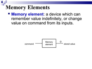


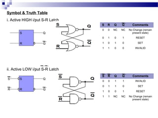

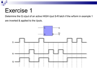


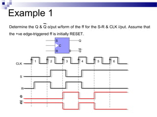
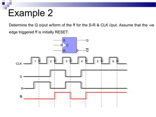

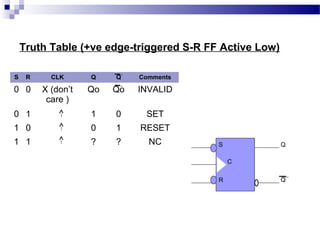


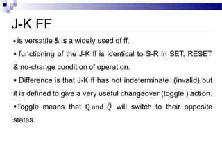
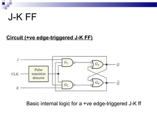
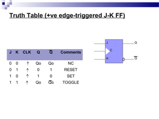


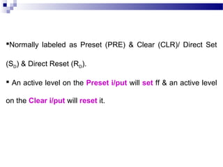

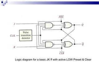


This document discusses sequential logic circuits and memory elements. It describes latches and flip-flops, which are basic memory elements used in sequential circuits. Specifically, it covers the set-reset (SR) latch, D flip-flop, and JK flip-flop. It provides their logic diagrams, truth tables, and examples of how their output changes in response to different input patterns over time. Asynchronous preset and clear inputs are also discussed as additional control inputs for flip-flops.


![16148_flip-flopaaaaaaaaaaaaaaaaa1[1].ppt](https://cdn.slidesharecdn.com/ss_thumbnails/16148flip-flop11-241007142703-8f186e77-thumbnail.jpg?width=640&height=640&fit=bounds)


