Downloaded 135 times
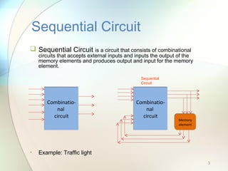
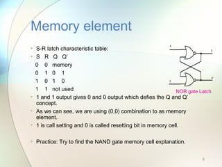
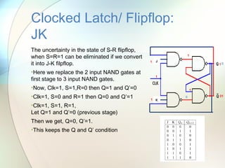
![• The basic memory element of a digital system is known as a latch or
flip-flop.
• A flip-flop or latch is made of NAND or NOR gate.
• Considering the NOR gate latch:
• Truth table:
• A B Out
0 0 1
0 1 0
1 0 0
1 1 0 [prohibited in memory cells]
• In the figure, S=Set and R=Reset.
• Let, S=1, R=0 then Q’=0 and Q=1.
Memory element
4
NOR gate Latch
NAND gate Latch
=1
=0
0
1
0
11
This is also known as S-R Latch.](https://image.slidesharecdn.com/sequentialcircuit-160104110221/85/Sequential-circuit-Digital-Electronics-4-320.jpg)
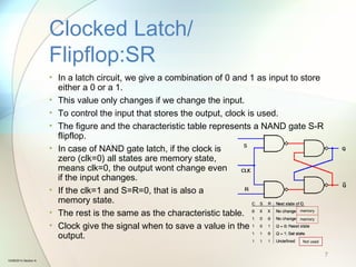
![• Truth table:
• A B Out
0 0 1
0 1 0
1 0 0
1 1 0 [prohibited in memory cells]
• Let, S=0, R=0 then, Q’=0 and Q=1
• Let Again, R=1, S=0 then Q’=1 and Q=0
• Let Again, S=0, R=0 then Q’=1 and Q=0
• This represents that,
current output is
dependent on previous
output.
Memory element
5
NOR gate Latch
1
=0
=0
00
1
NOR gate Latch
1
0
01
00
00
0
0
1](https://image.slidesharecdn.com/sequentialcircuit-160104110221/85/Sequential-circuit-Digital-Electronics-5-320.jpg)

This document discusses sequential circuits and memory elements. It explains that sequential circuits contain memory elements like latches and flip-flops that accept inputs and use previous outputs to produce new outputs. Common memory elements are S-R latches made from NOR or NAND gates, with truth tables defining their behavior. Clocked flip-flops like D and J-K flip-flops were introduced to control input storage using a clock signal.