Downloaded 368 times
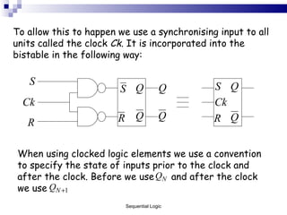
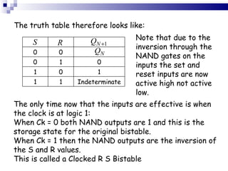
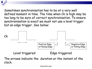
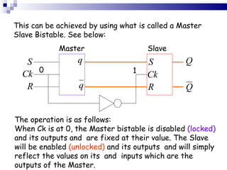
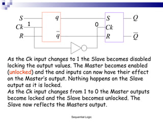
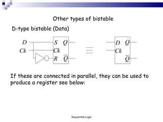
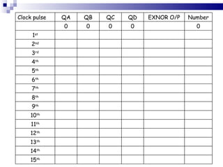
The document outlines sequential logic systems as part of the digital logic and signal principles module at the University of Wales Newport. It highlights the importance of sequential logic in engineering, detailing components like bistable circuits and their applications in digital systems, such as storage elements and registers. The material serves as an educational resource for developing practical skills in sequential logic and its implementation in engineering contexts.