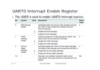
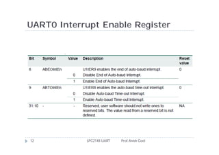
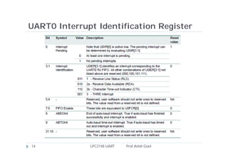
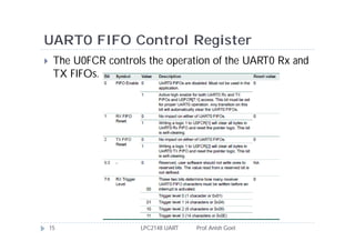
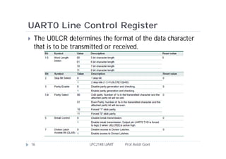
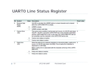
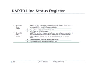
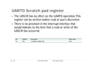
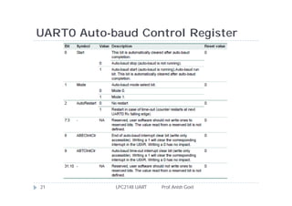
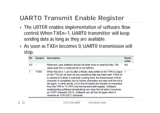
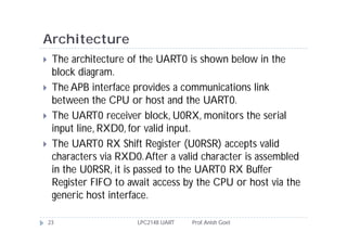
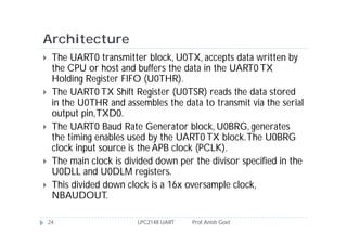
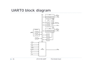
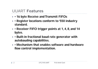
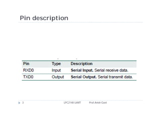
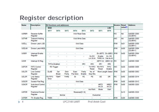
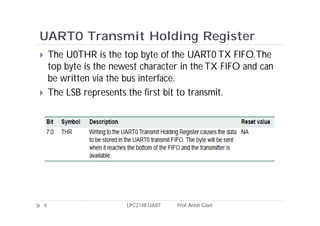
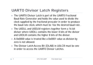
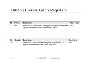
The document describes the features and architecture of the UART0 block in the ARM LPC2148 microcontroller. It has 16-byte transmit and receive FIFOs and supports standard UART features like baud rate generation and interrupts. The architecture uses separate transmit and receive shift registers connected to the transmit and receive FIFOs. A baud rate generator divides the system clock to generate the baud clock.

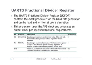
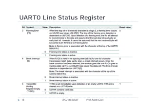
![Baud Rate Calculation
Where PCLK is the peripheral clock, U0DLM and U0DLL
are the standard UART0 baud rate divider registers, and
DIVADDVAL and MULVAL are UART0 fractional
baudrate generator specific parameters.
[Refer Section 10.3.5 of UM2148 for standard baudrate
calculation]
10 LPC2148 UART Prof. Anish Goel](https://image.slidesharecdn.com/llpc2148sci-110729020010-phpapp01/85/Llpc2148-sci-10-320.jpg)