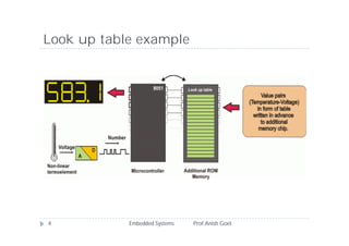
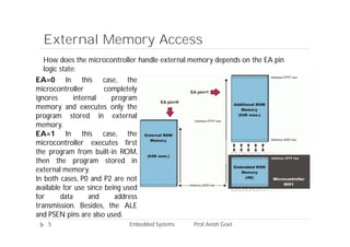
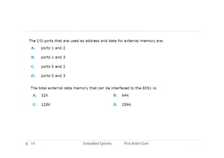
8051 Microcontroller
Memory Organization
Prof. Anish Goel
Embedded Systems
Memory Organization
Embedded Systems Prof.Anish Goel2
 The 8051 has two types of memory and these are
Program Memory and Data Memory.
 Program Memory (ROM) is used to permanently save the
program being executed, while Data Memory (RAM) is
used for temporarily storing data and intermediate results
created and used during the operation of the
microcontroller.
 Depending on the model in use at most a few Kb of ROM
and 128 or 256 bytes of RAM is used.
 All 8051 microcontrollers have a 16-bit addressing bus
and are capable of addressing 64 kb memory.
Program Memory
Embedded Systems Prof.Anish Goel3
 The first models of the 8051 microcontroller family did not have
internal program memory.
 It was added as an external separate chip.
 These models are recognizable by their label beginning with 803 (for
example 8031 or 8032).
 All later models have a few Kbyte ROM embedded.
 Even though such an amount of memory is sufficient for writing
most of the programs, there are situations when it is necessary to
use additional memory as well.
 A typical example are so called lookup tables.
 They are used in cases when equations describing some processes
are too complicated or when there is no time for solving them.
 In such cases all necessary estimates and approximates are executed
in advance and the final results are put in the tables (similar to
logarithmic tables).
Look up table example
Embedded Systems Prof.Anish Goel4
External Memory Access
Embedded Systems Prof.Anish Goel5
How does the microcontroller handle external memory depends on the EA pin
logic state:
EA=0 In this case, the
microcontroller completely
ignores internal program
memory and executes only the
program stored in external
memory.
EA=1 In this case, the
microcontroller executes first
the program from built-in ROM,
then the program stored in
external memory.
In both cases, P0 and P2 are not
available for use since being used
for data and address
transmission. Besides, the ALE
and PSEN pins are also used.
Data Memory
Embedded Systems Prof.Anish Goel6
 Data Memory is used for temporarily storing data and
intermediate results created and used during the operation of
the microcontroller.
 Besides, RAM memory built in the 8051 family includes many
registers such as hardware counters and timers, input/output
ports, serial data buffers etc.
 The previous models had 256 RAM locations, while for the
later models this number was incremented by additional 128
registers.
 However, the first 256 memory locations (addresses 0-FFh)
are the heart of memory common to all the models belonging
to the 8051 family.
 Locations available to the user occupy memory space with
addresses 0-7Fh, i.e. first 128 registers. This part of RAM is
divided in several blocks.
Data Memory
Embedded Systems Prof.Anish Goel7
 The first block consists of 4 banks each including 8 registers
denoted by R0-R7.
 Prior to accessing any of these registers, it is necessary to
select the bank containing it.
 The next memory block (address 20h-2Fh) is bit- addressable,
which means that each bit has its own address (0-7Fh).
 Since there are 16 such registers, this block contains in total of
128 bits with separate addresses (address of bit 0 of the 20h
byte is 0, while address of bit 7 of the 2Fh byte is 7Fh).
 The third group of registers occupy addresses 2Fh-7Fh, i.e. 80
locations, and does not have any special functions or features.
Memory expansion
Embedded Systems Prof.Anish Goel8
 In case memory (RAM or ROM) built in the
microcontroller is not sufficient, it is possible to add two
external memory chips with capacity of 64Kb each. P2
and P3 I/O ports are used for their addressing and data
transmission.
External Memory Interface
Embedded Systems Prof.Anish Goel9
External Memory Interface
Embedded Systems Prof.Anish Goel10
 From the user’s point of view, everything works quite
simply when properly connected because most
operations are performed by the microcontroller itself.
 The 8051 microcontroller has two pins for data read
RD#(P3.7) and PSEN#.
 The first one is used for reading data from external data
memory (RAM), while the other is used for reading data
from external program memory (ROM).
 Both pins are active low. A typical example of memory
expansion by adding RAM and ROM chips is shown in
figure above.
External Memory Interface
Embedded Systems Prof.Anish Goel11
 When the program during execution encounters an instruction
which resides in external memory (ROM), the microcontroller will
activate its control output ALE and set the first 8 bits of address
(A0-A7) on P0. IC circuit 74HCT573 passes the first 8 bits to
memory address pins.
 A signal on the ALE pin latches the IC circuit 74HCT573 and
immediately afterwards 8 higher bits of address (A8-A15) appear on
the port. In this way, a desired location of additional program
memory is addressed. It is left over to read its content.
 Port P0 pins are configured as inputs, the PSEN pin is activated and
the microcontroller reads from memory chip.
 Similar occurs when it is necessary to read location from external
RAM. Addressing is performed in the same way, while read and write
are performed via signals appearing on the control outputs RD (is
short for read) orWR (is short for write).
ICE BREAKER
Embedded Systems Prof.Anish Goel12
Embedded Systems Prof.Anish Goel13
Embedded Systems Prof.Anish Goel14
Embedded Systems Prof.Anish Goel15

Embedded systems ppt iii

  • 1.
  • 2.
    Memory Organization Embedded SystemsProf.Anish Goel2  The 8051 has two types of memory and these are Program Memory and Data Memory.  Program Memory (ROM) is used to permanently save the program being executed, while Data Memory (RAM) is used for temporarily storing data and intermediate results created and used during the operation of the microcontroller.  Depending on the model in use at most a few Kb of ROM and 128 or 256 bytes of RAM is used.  All 8051 microcontrollers have a 16-bit addressing bus and are capable of addressing 64 kb memory.
  • 3.
    Program Memory Embedded SystemsProf.Anish Goel3  The first models of the 8051 microcontroller family did not have internal program memory.  It was added as an external separate chip.  These models are recognizable by their label beginning with 803 (for example 8031 or 8032).  All later models have a few Kbyte ROM embedded.  Even though such an amount of memory is sufficient for writing most of the programs, there are situations when it is necessary to use additional memory as well.  A typical example are so called lookup tables.  They are used in cases when equations describing some processes are too complicated or when there is no time for solving them.  In such cases all necessary estimates and approximates are executed in advance and the final results are put in the tables (similar to logarithmic tables).
  • 4.
    Look up tableexample Embedded Systems Prof.Anish Goel4
  • 5.
    External Memory Access EmbeddedSystems Prof.Anish Goel5 How does the microcontroller handle external memory depends on the EA pin logic state: EA=0 In this case, the microcontroller completely ignores internal program memory and executes only the program stored in external memory. EA=1 In this case, the microcontroller executes first the program from built-in ROM, then the program stored in external memory. In both cases, P0 and P2 are not available for use since being used for data and address transmission. Besides, the ALE and PSEN pins are also used.
  • 6.
    Data Memory Embedded SystemsProf.Anish Goel6  Data Memory is used for temporarily storing data and intermediate results created and used during the operation of the microcontroller.  Besides, RAM memory built in the 8051 family includes many registers such as hardware counters and timers, input/output ports, serial data buffers etc.  The previous models had 256 RAM locations, while for the later models this number was incremented by additional 128 registers.  However, the first 256 memory locations (addresses 0-FFh) are the heart of memory common to all the models belonging to the 8051 family.  Locations available to the user occupy memory space with addresses 0-7Fh, i.e. first 128 registers. This part of RAM is divided in several blocks.
  • 7.
    Data Memory Embedded SystemsProf.Anish Goel7  The first block consists of 4 banks each including 8 registers denoted by R0-R7.  Prior to accessing any of these registers, it is necessary to select the bank containing it.  The next memory block (address 20h-2Fh) is bit- addressable, which means that each bit has its own address (0-7Fh).  Since there are 16 such registers, this block contains in total of 128 bits with separate addresses (address of bit 0 of the 20h byte is 0, while address of bit 7 of the 2Fh byte is 7Fh).  The third group of registers occupy addresses 2Fh-7Fh, i.e. 80 locations, and does not have any special functions or features.
  • 8.
    Memory expansion Embedded SystemsProf.Anish Goel8  In case memory (RAM or ROM) built in the microcontroller is not sufficient, it is possible to add two external memory chips with capacity of 64Kb each. P2 and P3 I/O ports are used for their addressing and data transmission.
  • 9.
    External Memory Interface EmbeddedSystems Prof.Anish Goel9
  • 10.
    External Memory Interface EmbeddedSystems Prof.Anish Goel10  From the user’s point of view, everything works quite simply when properly connected because most operations are performed by the microcontroller itself.  The 8051 microcontroller has two pins for data read RD#(P3.7) and PSEN#.  The first one is used for reading data from external data memory (RAM), while the other is used for reading data from external program memory (ROM).  Both pins are active low. A typical example of memory expansion by adding RAM and ROM chips is shown in figure above.
  • 11.
    External Memory Interface EmbeddedSystems Prof.Anish Goel11  When the program during execution encounters an instruction which resides in external memory (ROM), the microcontroller will activate its control output ALE and set the first 8 bits of address (A0-A7) on P0. IC circuit 74HCT573 passes the first 8 bits to memory address pins.  A signal on the ALE pin latches the IC circuit 74HCT573 and immediately afterwards 8 higher bits of address (A8-A15) appear on the port. In this way, a desired location of additional program memory is addressed. It is left over to read its content.  Port P0 pins are configured as inputs, the PSEN pin is activated and the microcontroller reads from memory chip.  Similar occurs when it is necessary to read location from external RAM. Addressing is performed in the same way, while read and write are performed via signals appearing on the control outputs RD (is short for read) orWR (is short for write).
  • 12.
  • 13.
  • 14.
  • 15.