Have you ever wondered how devices talk to each other? The answer might lie in a seemingly basic, yet incredibly effective protocol called UART, I want to share here what I learnt through my little journey of designing and testing UART.
Two devices havingdifferent internal clocks
efficiently exchange large amounts of data using
a simple two-wire connection and no separate
signals to mark the start and end of
transmission, How do they do it?
3.
What mechanism enableasynchronous data
transfer between devices with independent clock
domains, using just two wires and no dedicated
framing signals for start and end of
transmission?
ASYNC VS
SYNC
COMMUNICATION
Basically, theyboth share the same principle
where the receiver must be aware of when the
transmitter starts and when it completes its
data transfer process.
Asynchronous Synchronous
Synchronous communication requires that the
clocks in the transmitting and receiving devices
are synchronized
Receiving and transmitting devices don’t share
the same clock.
The resynchronization is accomplished using a
“START” symbol while the units of transmission
are framed between a “START” and “STOP”
symbol.
7.
UART
HARDWARE COMPLEXITY
UART generallyhas the least
hardware complexity comparing
to synchronous communication
protocols like I2C and SPI
FULL DUPLEX COMMUNICATION
UART's power consumption is
typically lower than that of SPI
and I2C.
POWER CONSUMPTION
UART can send and receive data
during the same clock cycle.
8.
If there isno data transmitter will
always send a signal usually(1).
Otherwise, it starts its sequence by
sending a different signal (0) so that the
receiver knows that the transmitter is
sending data now.
This 0 bit lunches the receiver sequence.
the form of data frames sent and the
speed at which it’s sent is agreement
between receiver and transmitter
WORKING PRINCIPLE
This’ll be discussed further in these slides
9.
Takes bytes ofdata and transmits
the individual bits in a sequential
fashion.
At the destination, a second UART
re-assembles the bits into complete
bytes.
WORKING PRINCIPLE
TRANSMITTER
RECEIVER
10.
Problem:
The Receiver andTransmitter devices often have
different clock frequencies.
So the receiver can miss the start bit or even
multiple data frame bits.therefore,they both must
be synchronised.
Solution:
For data to be transmitted correctly between devices
with different clock frequencies, the receiver must
sample the data at the same rate at which the
transmitter is sending it.
we often use clock dividers in UARTs. These dividers act
like gears, reducing the speed of a higher-frequency
clock signal to a value closer to the transmitter's baud
rate (data transmission speed)
To do so we us clock dividers to match the receiver's
sampling rate to the transmitter's baud rate for
accurate data reception.
Example:
2 Microcontrollers transferring
using UART protocol:
UART1 operates at 10MHz
UART2 operates at 5MHz
WORKING PRINCIPLE #1
If we want them both to send and receive at
1MHz (10^6 bit/sec)
we must use the correct divider for
each device.
So by applying 1010 binary (10 decimal) to
UART1's clock divider and 0101(5) to UART2's
clock divider we get the same transmitting and
receiving rate.
11.
Applying divider valuesfor 2 UART modules to make them send and receive at the same rate
Baud Rate Generator ”Clock Divider”
Baud Rate Generator ”Clock Divider”
A packet consistsof a start bit, data frame
a parity bit and stop bits.
Problem:
Although now both transmitter and receiver are
running at the same rate because of the
configurable clock generator in both devices, the
data still won’t be transferred in correct manner.
Solution:
Unless the data is being sent in particular order
and in fixed size that the 2 parties agree on, the
receiver will catch different data from the one
sent.
Therefore, packets are used in data transmission
WORKING PRINCIPLE #2
UART packet.
In discussed design here:
when UART Transmitter is enabled it
sends the start bit first (start bit is 0).
After that it sends the data in series
(8bits).
Then if parity generator is enabled it
sends the parity bit(notice that both
UART modules must support parity bit in
this case).
After Parity bit or in case it’s not
supported the transmitter sends the
stop bit which equals the IDLE bit (both
are 1).
14.
IDLE Bit Value1
Start Bit Value 0
Data Frame Width 8
Parity Bit Optional
Stop Bit Value 1
The Receiver Is FSM(Finite State Machine)
it has finite number of states (idle, start, data,
parity, stop), which can be encoded using gray code,
binary code or one-hot encoding and stored in
register.
at beginning as long as the transmitter is sending 1
the receiver’s state is IDLE.
when transmitter sends the start bit (0)
the receiver detect that and changes its state
to start.
now the receiver knows that next 8 bits are data.
If parity generation is enabled, then after sampling
the 8 bits, the receiver verifies the data using this
parity bit through the
“Parity Checker“ module inside the receiver.
And finally receiving the stop bit followed by
returning to the Idle state (now it’s ready to receive
another packet)
WORKING PRINCIPLE #2
In discussed design here:
BAUD RATE
GENERATOR
It takesthe system clock and divider as input.
It uses counter to divide the clock to the desired
rate.
Counter increases every clock cycle and it’s reset to zero
when counter value equal the input divider value - 1 .
Output is high when Counter equals 1
FUNCTIONALITY:
1
SERIALIZER &
PARITY GENERATOR
ParityGenerator
both take input data and valid signal.
both have 8-bit internal memory.
when valid signal is high the input data is loaded in
memory
In Parity Generator the stored data is connected to XOR
gate(even parity bit) the result then split, one part is
connected to mux and other is connected to inverter(odd
parity bit), the mux selector is “parityType” signal the
output is either odd parity bit or even parity bit.
FUNCTIONALITY:
INPUT/OUTPUT:
24.
PARITY
CALCULATOR
VERILOG CODE
ParitCalculator.v
memory isused to make the
result more reliable and
independent from the input.
“dataValid” signal must be high
for only one cycle.
“dataValid” is set high to lunch
transmitter sequence and store
the input data (in
parityCalculator and Serializer).
2
MSB LSB Out
SERIALIZER&
PARITY GENERATOR
Serializer
In Serializer the data is stored in shift register and the 8-
bit shift register that its output is connected to 1-bit
register, when transmitter next state is data the FSM
enable the data serializer for one cycle.
Next, it enable it again every 1/(Baud Rate)
sec(transmitting rate).
Every time the SerializerEnable signal is high the LSB in
data is moved to ouput register and the data in memory is
right shifted and “ptr” register increases by 1
“SerializerDone” =(“ptr”==8)
27.
SERIALIZER
VERILOG CODE
Serializer.v
“dataValid” isused here also for the
same reasons discussed previously.
Shifter right shifts the data bits only
when “serializerEn” is high.
This is how FSM unit controls the shifting
process (shift bit every (1/baud rate)sec
to output register), this’ll be discussed
further in the following slides.
Another thing is “SerializerDn” which is
how Serializer tells the controller “I’ve
finished shifting all data bits to output.
28.
FSM unit (thecontroller unit) controls:
Timing
manages the on/off state timing of the enable signal.
FSM activate “En” for one clock cycle every (1/baud rate) sec therefore it
shifts only bit every determine bit period (1/baud rate).
handles the timing of switching between different inputs on the mux
Sequence
manages the order in which data is sent through the selector.
MSB LSB Out
FSM
MUX
COMPARATOR
(==8)
TRANSMITTER
FSM UNIT(CONTROLLER)
DIAGRAM
En
Tx Out
Ptr
Selector
Done
29.
Current
value
b000 b001 b010b011 b100
Mux Output IDLE bit(1)
Start
bit(b0)
Connected to
serializer
Connected to Parity
Calculator
Stop bit(b1)
TRANSMITTER
FSM UNIT(CONTROLLER)
DIAGRAM
Every state is binary encoded and
store in 3-bit register(“Current”):
IDLE: b000
START: b001
DATA: b010
PARITY: b011
STOP: b100
In the discussed design the Mux
Selector is connected to “Current”
register output.
30.
Oversampling Common values
4
8
16
Discussionabout BAUD Generator Output & UART Baud Rate #1
In the UART design here, the baud generator doesn't directly determine the speed of data
transfer (bit/s).
Instead, the baud generator's output’s frequency is divided by 16(OVERSAMPLING)
within the receiver (FSMRX) and transmitter (FSMTX) by counters called "baud counters".
The final result is the true baud rate as you will see in the upcoming slides.
Note that oversampling constant can be any number but
it’s recommended to be even number.
31.
Discussion about BAUDGenerator Output & UART Baud Rate #1
This equation helps us find the correct value for the divider (DIV) used by
the baud rate generator. This ensures we achieve the desired baud rate for communication.
The reasons why the “oversampling” term is used in this equation will be
discussed further in the following slides
1. Decide the proper baud rate for UART communication;
2.Calculate the divider that brings system clock down to the desired baud rate.
Reminder: The Baud Rate Generator’s output clock is Hz only.
Another frequency dividers in both receiver and transmitter will
divide down this frequency by OVERSAMPLING constant(16x,8x or 4x) to the wanted baud rate.
32.
Can’t we justuse this equation
to divide down the system clock to desired frequency?
the answer is yes we can, but the problem hasn’t ever been
here(Transmitter).
So, what is the purpose of another divider??
Notice that we always wait for the BaudCounter To reach 16.
“Baud” counter is used to divide the Baud Rate Generator output
but Why????
TRANSMITTER
FSM UNIT(CONTROLLER)
DIAGRAM
33.
To do sowe need to establish sampling point once at the middle
of start bit period and then samples data every
(1/baud rate) sec
“Establishing a sampling point that is near the middle of the bit
period” is the answer for previous question .
WHY DON’T WE USE
ONLY BAUD RATE
GENERATOR TO GET THE
EXACT FREQUENCY WE
NEED?
for optimum robust against clock-frequency differences,
we samples the transmitted data bits at the midpoint of their
period.
34.
WHY DON’T WEUSE
ONLY BAUD RATE
GENERATOR TO GET THE
EXACT FREQUENCY WE
NEED?
Start Bit Sampling: Ideally, the receiver should establish
sample point at the mid of the start bit. This requires a
sampling clock with a frequency twice the baud rate (data bits
per second) of the transmission. (In other words, the sampling
period would be half the bit time.)
Data Bit Sampling: For the remaining data bits within the
packet, the receiver typically samples the signal whenever the
baud rate generator output is high. This is because a high
output from the baud rate generator usually indicates the
data transmission period within a bit time.
Div is configured by user so it’s not predictable, in order to
get twice the baud rate we will need divider.
35.
A WAY TOESTABLISH
SAMPLING POINT BUT IT
REQUIRES AN
ARITHMETIC DIVIDER.
36.
ANOTHER WAY TO
ESTABLISHSAMPLING
POINT IT REQUIRES ONLY
ANOTHER FREQUENCY
DIVIDER (COUNTER).
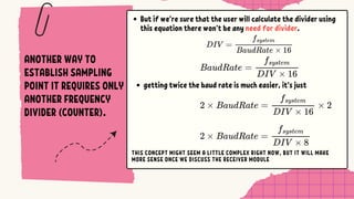
But if we’re sure that the user will calculate the divider using
this equation there won’t be any need for divider.
getting twice the baud rate is much easier, it’s just
THIS CONCEPT MIGHT SEEM A LITTLE COMPLEX RIGHT NOW, BUT IT WILL MAKE
MORE SENSE ONCE WE DISCUSS THE RECEIVER MODULE
Discussion about OVERSAMPLINGParameter
The OVERSAMPLING in the discussed design here is not really related to over-sampling method.
that’s because the receiver is taking only one sample at midpoint within each bit time
(Standard Sampling) rather than taking multiple samples and use these samples to distinguish
between data and noise spikes(Oversampling),
Testbench Parameters, Stimuliand Output Signals
TX_TOP.v
These are our TB local parameters(constants)
DATAWIDTH: serializer shift register width, the maximum ptr value at which serializer’s done
flag is set high.
PERIOD: This is System Clock Period in nano seconds It takes 10 ns to complete one
cycle(100Mhz).
41.
Testbench Parameters, Stimuliand Output Signals
TXTOP_TB.v
These are TB Stimuli
parityEnable: tells the transmitter whether to send data parity bit or no if so it’ll
generate parity bit for the input data.
parity type: tells the transmitter whether to generate even parity bit (0) or odd
parity bit(1).
tx_input_tb: this is transmitter input; the input data is parallel it’s coming from the
device to which UART connected.
DIV: baud rate generator’s input signal (divider value ).
TXTOP_TB.v
42.
Testbench Parameters, Stimuliand Output Signals
TX_TOP.v
These are TB Output Signals
tx_tb: the transmitter output data.
tx_done_tb: Is high when the transmitter next state is IDLE.
mData: used to verify the function of transmitter by collecting the data from transmitter and comparing it
with the input.
mPacket: used to display the whole packet in order (the msb represent the idle bit before the start bit and lsb
represent the last bit in the packet).
Note:
Serializer in transmitterUART outputs data starting from LSB to MSB,
So this data frame: 11001100 is sent reversed: 00110011.
Testbench Strategy:
1-Assign 8 parallel bits to UART transmitter.
TXTOP_TB.v
Important Note:
if we set parity enable we must make sure that the receiver’s parity checker is enabled.
Parity Enable Parity Type
45.
2-Write verilog codeto collect the transmitted data in one variable,
so that we can verify the transmitter functionality later
TXTOP_TB.v
MSB LSB
tx_t
b
mData
46.
Expected Output (mPacket):
IDLE0000(0)
START 0001(1)
DATA 0010(2)
PARITY 0011(3)
STOP 0100(4)
Note that the transmitter states is binary encoded like this:
Transmitter
State
(Current)
IDLE Start Data Data Data Data Data Data Data Data Parity Stop IDLE
Bit Value 1 0
LSB
(1)
1 1 1 0 1 1
MSB
(1)
1 1 1
Bit Order 1 2 3 4 5 6 7 8 9 10 11 12 13
mPacket
47.
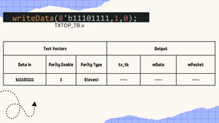
Test Vectors Output
DataIn Parity Enable Parity Type tx_tb mData mPacket
b11101111 1 0(even) ---- ---- ----
TXTOP_TB.v
48.
you can seethat at beginning:
dataValid_tb is 0 for some time then it becomes high for one cycle and the following
happen:
load the input data in transmitter registers.
initialize the transmitting process(IDLE->START)
Current (transmitter state):
changes from IDLE to START
tx_tb:
when Current changes to START, the transmitter outputs the start through the
Test Beginning:
49.
Every bit hasperiod of (System Clock Period *Baud Rate Generator (DIV) *
OVERSAMPLING)
Start bit: 0 bit1: 1
After baud rate period(bit period) from the beginning of Start bit.
The transmitter’s FSM unit enables serializer.
The transmitter’s next state becomes DATA.
The Baud Counter next value is zero.
One cycle later:
value of next state signal is assigned to Current and it becomes DATA.
Baud Counter is reset.
50.
During PARITY Statethe transmitter ‘s output is the parity bit.
11110111 should generate even parity bit of 1.
Every bit has period of (System Clock Period *Baud Rate Generator (DIV) *
OVERSAMPLING).
The Data bits Are 11110111 (7 highs).
After Sampling data bits transmitters state is changed to PARITY
Start bit: 0 bit1: 1 bit2: 1 bit3: 1 bit4: 1 bit5: 0 bit6: 1 bit7: 1 bit8: 1
Even Parity bit(high)
51.
At the endtransmitter State becomes STOP and it changes selector
to send stop bit, when the receiver samples the stop bit if it’s not
1(high), a framing error is flagged.
Stop bit (high)
Notice that mData is 11101111 which is same as the input data.
mPacket is 10111101111 .
Bit Value
1
IDLE
0
Start
(1) 1 1 1 0 1 1 (1)
1
Parity
1
Stop
1
IDLE
Bit Order 1 2 3 4 5 6 7 8 9 10 11 12 13
52.
Test Vectors Output
DataIn Parity Enable Parity Type mData mPacket
11101111 1 0(even) 11101111 101111011111
TESTBENCH PASSED
(STOP) (IDLE)
tx_done_tb is high: this can be used to read next packet from FIFO
memory.
DESERIALIZER
PARITY CHECKER
The deserializeracts as the counterpart to the
serializer. It takes a serial data stream (one bit at a
time) and reconstructs the original parallel data.
It do so by storing it in shift register bit by bit at the
end when shift register pointer’s value reaches data
frame width (8) the “deserializerDone” flag is set high
telling FSM unit to move to next state (parity or stop).
Parity Checker takes the data from deserializer and
generate its parity bit then compare it with the one
came from transmitter .
If they don’t match a parity error is flagged.
55.
FSM (CONTROLLER)
FSM inreceiver is similar to the one in transmitter but
instead of moving to start when “dataValid” signal is high
it moves to start when it detects the start bit (0) on input
port (rx).
Another thing is that the baud Counter counts only to 8
before the it allow the FSM state to move from start to
data. but for the remain transitions it takes the baud
counter to reach 16 first before it happens,
56.
01 02
To improveaccuracy, the receiver takes
samples of the data bits at their center
points, reducing the chance of errors
Notice that the design may still work if we
sample data at the edge of every bit period.
Testbench Parameters, Stimuliand Output Signals
RX_TOP.v
These are our TB local parameters(constants)
DATAWIDTH: deserializer shift register width, the maximum ptr value at which deserializer’s
done flag is set high.
OVERSAMPLING: we don’t sample any bit before baud generator output clock is high
“OVERSAMPLING” times then reset the baud counter and wait the same amount of time to
sample the next bit (we do so till the stop bit).
PERIOD: This is System Clock Period in nano seconds It takes 10 ns to complete one
cycle(100Mhz).
60.
OVERSAMPLING
in receiver alsothe baud counter is used to divide the
baud generator frequency down by OVERSAMPLING to
the desired UART Baud Rate.
61.
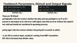
Testbench Parameters, Stimuliand Output Signals
RXTOP_TB.v
These are TB Stimuli
parityEnable: tells the receiver whether the data sent has paritybit or no if so it’ll
process it and output error and error valid signal, note that an error without this signal is
not valid and should not considered in upcoming proccess.
parity type: tells the receiver whether the parity bit is even(0) or odd(1).
rx_tb: this is receiver input, usually it’s coming from UART transmitter.
DIV: this is the baud clock divider value.
RXTOP_TB.v
62.
Testbench Parameters, Stimuliand Output Signals
RXTOP_TB.v
These are TB Output Signals
rx_out_tb: the receiver output data
pCheckErrorOut_tb: the receiver’s parity checker error flag
pCheckValidOut_tb:
the receiver’s parity checker error valid signal.
It’ll only active when parity checking is enabled (parEn is on).
Helps connected devices determine if the error should be considered or ignored.
rx_done: Is high when the next state is idle that means that a whole
packet [(start, data, parity, stop)bits] has been received
(can be used to store data in FIFO when the receiving is done).
1->IDLE, 0->Start bit,[1->LSB, 1001101->rest of data] , 1->Stop bit
Note:
Serializer in transmitter UART outputs data starting from LSB to MSB,
So this data frame: 11001100 that’s sent by transmitter is actually 00110011.
Testbench Strategy:
1-Sends 11 individual bits (packet)[IDLE bit(1), Start bit(0), Data(8 bits)[LSB->MSB], Parity(1/0), Stop bit(1)]
RX_TOP.v
Important Note:
the second and third parameters in “sendData” task is parity enable and parity type
if we set parity enable we must make sure that between start and end bit
there are 9 bits: 8 for data frame and one parity bit.
65.
2-then make surethat every bit has a period of 1/(Baud Rate) sec,
which is the same rate at which UART Receiver samples the data .
0->DATAWIDTH-1: 8bits
0->((DATAWIDTH-1)+3): 8bits + Start bit + Stop bit +IDLE bit
0->((DATAWIDTH-1)+3)+1: one more bit for potential Parity bit
RX_TOP.v
66.
Testbench Parameters, Stimuliand Output Signals
RX_TOP.v
These are TB Output Signals
rx_out_tb: the receiver output data
pCheckErrorOut_tb: the receiver’s parity checker error flag
pCheckValidOut_tb:
the receiver’s parity checker error valid signal.
It’ll only active when parity checking is enabled (parEn is on).
Helps connected devices determine if the error should be considered or ignored.
rx_done: Is high when the next state is idle that means that a whole packet [(start, data, parity,
stop)bits] has been received (can be used to store data in FIFO when the receiving is done).
framingError_tb: Is set high when the stop bit doesn’t equal.
67.
Test Vectors Output
DataIn
Parity
Enable
Parity Type rx_out_tb
pCheckValidO
ut_tb
pCheckError
Out_tb
framingError
b101100110111 1 0(even) ---- ---- ---- ----
Analyse Input:
IDLE Start Data Data Data Data Data Data Data Data Parity Stop
1 0
LSB
(1)
1 0 0 1 1 0
MSB
(1)
1 1
68.
Expected Output: 10110011
10 1 1 0 0 1 1
IDLE 0000(0)
START 0001(1)
DATA 0010(2)
PARITY 0011(3)
STOP 0100(4)
Note that the receiver states is binary encoded like this:
Parity Error Flag: 0
Parity Error Valid Flag: 0
Framing Error Flag: 0
69.
you can seethat at beginning:
The input is one and the output is zero.
Receiver state(Current) is IDLE(000).
All flags are low.
After That:
Receiver detects 0 bit therefore it moves to the next state(start).
when it reaches the middle of start bit it moves to the next state:
data (010).
70.
you can seethat at beginning:
The input is one and the output is zero.
Receiver state(Current) is IDLE(000).
All flags are low.
After That:
Receiver detects 0 bit therefore it moves to the next state(start).
when it reaches the middle of start bit it moves to the next state: data (010).
Sampling Stage:
The Receiver samples every bit at almost the middle of its period
the sampled bit is stored in receiver output register
Bit 1: 1 Bit 2: 1
71.
Receiver samples thelast data bit and after that the fsm(controller) receives high
“deserializerDn” flag from deserializer, the receiver moves then to next state (parity).
After that samples parity bit at the middle of its period after that it verify the data frame
using this parity bit in Parity Checker module.
If the received data parity bit doesn’t match this parity bit the error flag rises to 1 otherwise
it’s zero, and also since the “parEn” is high the error valid signal must be high also.
Bit 8: 1
Sampling Parity bit: 1
Notice the pCheckValidOut, it’s now high and the parity error is 0 so now we can take it for
granted that there is no parity error.
Bit 8: 1
paritybit stop bit
Baud Counter == 16
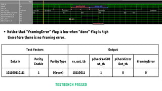
Notice that “framingError” flag is low when “done” flag is high
therefore there is no framing error.
Test Vectors Output
Data In
Parity
Enable
Parity Type rx_out_tb
pCheckValidO
ut_tb
pCheckError
Out_tb
framingError
101100110111 1 0(even) 10110011 1 0 0
TESTBENCH PASSED
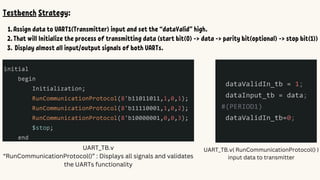
Testbench Strategy:
1.Assign datato UART1(Transmitter) input and set the “dataValid” high.
2.That will Initialize the process of transmitting data (start bit(0) -> data -> parity bit(optional) -> stop bit(1))
3. Display almost all input/output signals of both UARTs.
UART_TB.v
“RunCommunicationProtocol()” : Displays all signals and validates
the UARTs functionality
UART_TB.v( RunCommunicationProtocol() )
input data to transmitter
UART_TB.v( RunCommunicationProtocol() )
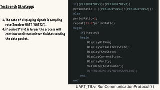
TestbenchStrategy:
1.
2.
3.The rate of displaying signals is sampling
rate(Receiver UART “UART2”).
4.if period1*div1 is larger the process will
continue until transmitter finishes sending
the data packet.
Transmitter UART ReceiverUART
System Clock Period 625ns 1250ns
Divider 10 5
Oversampling 16 16
Baud Rate 10000bit/s 10000bit/s
Test Vectors:
Parity
Transmitter input data Enable Type
b11011011 1 0(even)
11110001 1 0(even)
10000001 1 0(even)
This time is different, we will use RunCommunicationProtocol() to verify the design.
TEST:
Results:
86.
Transmitter UART ReceiverUART
System Clock Period 625ns 1250ns
Divider 10 10
Oversampling 16 16
Baud Rate 10000bit/s 5000bit/s
Test Vectors:
Parity
Transmitter input data Enable Type
b11011011 1 0(even)
11110001 1 0(even)
10000001 1 0(even)
This time is different, we will use RunCommunicationProtocol() to verify the design.
TEST:
Results:
88.
Transmitter UART ReceiverUART
System Clock Period 625ns 1250ns
Divider 15 10
Oversampling 16 16
Baud Rate 6666.67bit/s 5000bit/s
Test Vectors:
Parity
Transmitter input data Enable Type
b11011011 1 0(even)
11110001 1 0(even)
10000001 1 0(even)
This time is different, we will use RunCommunicationProtocol() to verify the design.
TEST:
Results:
90.
Transmitter UART ReceiverUART
System Clock Period 625ns(1.6 MHz) 1250ns(800kHz)
Divider 20 10
Oversampling 16 16
Baud Rate 5000bit/s 5000bit/s
Test Vectors:
Parity
Transmitter input data Enable Type
b11011011 1 0(even)
11110001 1 0(even)
10000001 1 0(even)
This time is different, we will use RunCommunicationProtocol() to verify the design.
TEST:
Results:


![BAUD RATE GENERATOR
DIV[11:0]
CLK
RST
BCLK](https://image.slidesharecdn.com/uart-250626024749-d37fac0b/85/UART-Verilog-Design-and-Testbench-Part-1-16-320.jpg)


![Testbench Parameters, Stimuli and Output Signals
RXTOP_TB.v
These are TB Output Signals
rx_out_tb: the receiver output data
pCheckErrorOut_tb: the receiver’s parity checker error flag
pCheckValidOut_tb:
the receiver’s parity checker error valid signal.
It’ll only active when parity checking is enabled (parEn is on).
Helps connected devices determine if the error should be considered or ignored.
rx_done: Is high when the next state is idle that means that a whole
packet [(start, data, parity, stop)bits] has been received
(can be used to store data in FIFO when the receiving is done).](https://image.slidesharecdn.com/uart-250626024749-d37fac0b/85/UART-Verilog-Design-and-Testbench-Part-1-62-320.jpg)

![1->IDLE, 0->Start bit, [1->LSB, 1001101->rest of data] , 1->Stop bit
Note:
Serializer in transmitter UART outputs data starting from LSB to MSB,
So this data frame: 11001100 that’s sent by transmitter is actually 00110011.
Testbench Strategy:
1-Sends 11 individual bits (packet)[IDLE bit(1), Start bit(0), Data(8 bits)[LSB->MSB], Parity(1/0), Stop bit(1)]
RX_TOP.v
Important Note:
the second and third parameters in “sendData” task is parity enable and parity type
if we set parity enable we must make sure that between start and end bit
there are 9 bits: 8 for data frame and one parity bit.](https://image.slidesharecdn.com/uart-250626024749-d37fac0b/85/UART-Verilog-Design-and-Testbench-Part-1-64-320.jpg)

![Testbench Parameters, Stimuli and Output Signals
RX_TOP.v
These are TB Output Signals
rx_out_tb: the receiver output data
pCheckErrorOut_tb: the receiver’s parity checker error flag
pCheckValidOut_tb:
the receiver’s parity checker error valid signal.
It’ll only active when parity checking is enabled (parEn is on).
Helps connected devices determine if the error should be considered or ignored.
rx_done: Is high when the next state is idle that means that a whole packet [(start, data, parity,
stop)bits] has been received (can be used to store data in FIFO when the receiving is done).
framingError_tb: Is set high when the stop bit doesn’t equal.](https://image.slidesharecdn.com/uart-250626024749-d37fac0b/85/UART-Verilog-Design-and-Testbench-Part-1-66-320.jpg)