SlideShare a Scribd company logo
Name of Subject Advanced Processor
Subject code 304189
Year 2020-21
Class TE E&Tc
Semester VI
Examination
Scheme
In-Sem(Paper)-30 Marks
End-Sem(Paper)-70 Marks
Unit no III
Name of Unit
Real World Interfacing with ARM7
Based Microcontroller-1
13-Sep-21 1
13-Sep-21 2
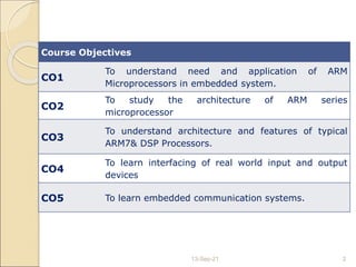
Course Objectives
CO1
To understand need and application of ARM
Microprocessors in embedded system.
CO2
To study the architecture of ARM series
microprocessor
CO3
To understand architecture and features of typical
ARM7& DSP Processors.
CO4
To learn interfacing of real world input and output
devices
CO5 To learn embedded communication systems.
13-Sep-21 3
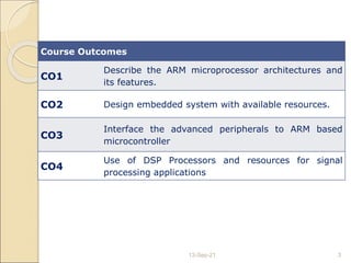
Course Outcomes
CO1
Describe the ARM microprocessor architectures and
its features.
CO2 Design embedded system with available resources.
CO3
Interface the advanced peripherals to ARM based
microcontroller
CO4
Use of DSP Processors and resources for signal
processing applications
Objectives
 UART(LPC2148)
 UART Register
13-Sep-21 4
UART(Universal Asynchronous
Receiver/Transmitter)
13-Sep-21 5
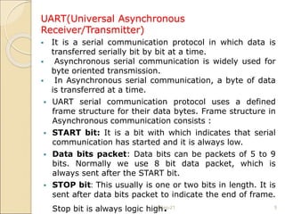
 It is a serial communication protocol in which data is
transferred serially bit by bit at a time.
 Asynchronous serial communication is widely used for
byte oriented transmission.
 In Asynchronous serial communication, a byte of data
is transferred at a time.
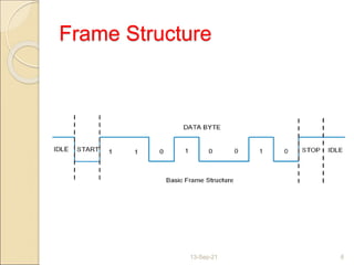
 UART serial communication protocol uses a defined
frame structure for their data bytes. Frame structure in
Asynchronous communication consists :
 START bit: It is a bit with which indicates that serial
communication has started and it is always low.
 Data bits packet: Data bits can be packets of 5 to 9
bits. Normally we use 8 bit data packet, which is
always sent after the START bit.
 STOP bit: This usually is one or two bits in length. It is
sent after data bits packet to indicate the end of frame.
Stop bit is always logic high.
Frame Structure
13-Sep-21 6
UART module
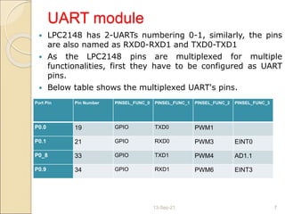
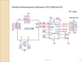
 LPC2148 has 2-UARTs numbering 0-1, similarly, the pins
are also named as RXD0-RXD1 and TXD0-TXD1
 As the LPC2148 pins are multiplexed for multiple
functionalities, first they have to be configured as UART
pins.
 Below table shows the multiplexed UART's pins.
13-Sep-21 7
Port Pin Pin Number PINSEL_FUNC_0 PINSEL_FUNC_1 PINSEL_FUNC_2 PINSEL_FUNC_3
P0.0 19 GPIO TXD0 PWM1
P0.1 21 GPIO RXD0 PWM3 EINT0
P0_8 33 GPIO TXD1 PWM4 AD1.1
P0.9 34 GPIO RXD1 PWM6 EINT3
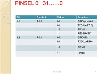
PINSEL 0 31……0
Bit Symbol Value Function
1:0 P0.0 00 GPIO port 0.0
01 TXD(UART 0)
10 PWM1
11 RESERVED
3:2 P0.1 00 GPIO P0.1
01 RXD(UART0)
10 PWM3
11 EINT0
13-Sep-21 8
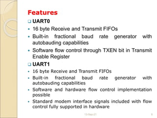
Features
 UART0
 16 byte Receive and Transmit FIFOs
 Built-in fractional baud rate generator with
autobauding capabilities
 Software flow control through TXEN bit in Transmit
Enable Register
 UART1
 16 byte Receive and Transmit FIFOs
 Built-in fractional baud rate generator with
autobauding capabilities
 Software and hardware flow control implementation
possible
 Standard modem interface signals included with flow
control fully supported in hardware
13-Sep-21 9
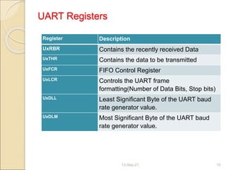
Register Description
UxRBR Contains the recently received Data
UxTHR Contains the data to be transmitted
UxFCR FIFO Control Register
UxLCR Controls the UART frame
formatting(Number of Data Bits, Stop bits)
UxDLL Least Significant Byte of the UART baud
rate generator value.
UxDLM Most Significant Byte of the UART baud
rate generator value.
13-Sep-21 10
UART Registers
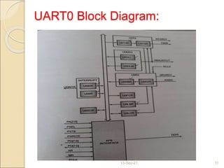
UART0 Block Diagram:
13-Sep-21 11
UART0 Registers
U0RBR (UART0 Receive Buffer Register)
 It is an 8-bit read only register.
 This register contains the received data.
 It contains the “oldest” received byte in the receive
FIFO.
 If the character received is less than 8 bits, the
unused MSBs are padded with zeroes.
 The Divisor Latch Access Bit (DLAB) in U0LCR must
be zero in order to access the U0RBR. (DLAB = 0)
13-Sep-21 12
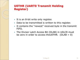
U0THR (UART0 Transmit Holding
Register)
 It is an 8-bit write only register.
 Data to be transmitted is written to this register.
 It contains the “newest” received byte in the transmit
FIFO.
 The Divisor Latch Access Bit (DLAB) in U0LCR must
be zero in order to access theU0THR. (DLAB = 0)
13-Sep-21 13
U0DLL and U0DLM (UART0 Divisor Latch
Registers)
 Both of them hold 8-bit values.
 These register together form a 16 bit divisor value
which is used in baud rate generation.
 U0DLM holds the upper 8 bits and U0DLL holds the
lower 8 bits and the formation is “[U0DLM:U0DLL].
 Since these form a divisor value and division by zero
is invalid,the starting for U0DLL is 0x01(not 0x00)i.e
starting value in combined formation is[0x00:0x01]
i.e.0x0001.
 In order to access and use these registers
properly,DLAB bit in U0LCR must be set to 1.
13-Sep-21 14
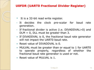
U0FDR (UART0 Fractional Divider Register)
• It is a 32-bit read write register.
• It decides the clock pre-scalar for baud rate
generation.
• If fractional divider is active (i.e. DIVADDVAL>0) and
DLM = 0, DLL must be greater than 3.
 If DIVADDVAL is 0, the fractional baud rate generator
will not impact the UART0 baud rate.
 Reset value of DIVADDVAL is 0.
 MULVAL must be greater than or equal to 1 for UART0
to operate properly, regardless of whether the
fractional baud rate generator is used or not.
 Reset value of MULVAL is 1.
13-Sep-21 15
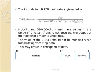
 The formula for UART0 baud rate is given below
 MULVAL and DIVADDVAL should have values in the
range of 0 to 15. If this is not ensured, the output of
the fractional divider is undefined.
 The value of the U0FDR should not be modified while
transmitting/receiving data.
 This may result in corruption of data.
13-Sep-21 16
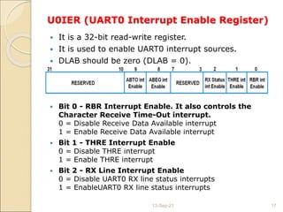
U0IER (UART0 Interrupt Enable Register)
 It is a 32-bit read-write register.
 It is used to enable UART0 interrupt sources.
 DLAB should be zero (DLAB = 0).
 Bit 0 - RBR Interrupt Enable. It also controls the
Character Receive Time-Out interrupt.
0 = Disable Receive Data Available interrupt
1 = Enable Receive Data Available interrupt
 Bit 1 - THRE Interrupt Enable
0 = Disable THRE interrupt
1 = Enable THRE interrupt
 Bit 2 - RX Line Interrupt Enable
0 = Disable UART0 RX line status interrupts
1 = EnableUART0 RX line status interrupts
13-Sep-21 17
 Bit 8 - ABEO Interrupt Enable
0 = Disable auto-baud time-out interrupt
1 = Enable auto-baud time-out interrupt
 Bit 9 - ABTO Interrupt Enable
0 = Disable end of auto-baud interrupt
1 = Enable the end of auto-baud interrupt
13-Sep-21 18
U0LCR (UART0 Line Control Register)
 It is an 8-bit read-write register.
 It determines the format of the data character that is
to be transmitted or received
13-Sep-21 19
13-Sep-21 20
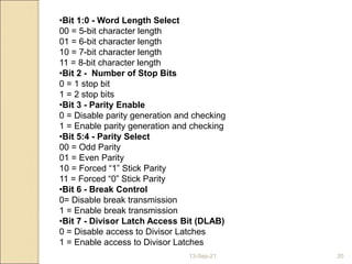
•Bit 1:0 - Word Length Select
00 = 5-bit character length
01 = 6-bit character length
10 = 7-bit character length
11 = 8-bit character length
•Bit 2 - Number of Stop Bits
0 = 1 stop bit
1 = 2 stop bits
•Bit 3 - Parity Enable
0 = Disable parity generation and checking
1 = Enable parity generation and checking
•Bit 5:4 - Parity Select
00 = Odd Parity
01 = Even Parity
10 = Forced “1” Stick Parity
11 = Forced “0” Stick Parity
•Bit 6 - Break Control
0= Disable break transmission
1 = Enable break transmission
•Bit 7 - Divisor Latch Access Bit (DLAB)
0 = Disable access to Divisor Latches
1 = Enable access to Divisor Latches
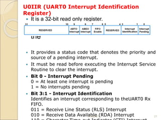
U0IIR (UART0 Interrupt Identification
Register)
 It is a 32-bit read only register.
 It provides a status code that denotes
the
 It provides a status code that denotes the priority and
source of a pending interrupt.
 It must be read before executing the Interrupt Service
Routine to clear the interrupt.
 Bit 0 - Interrupt Pending
0 = At least one interrupt is pending
1 = No interrupts pending
 Bit 3:1 - Interrupt Identification
Identifies an interrupt corresponding to theUART0 Rx
FIFO.
011 = Receive Line Status (RLS) Interrupt
010 = Receive Data Available (RDA) Interrupt
13-Sep-21 21
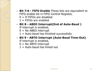
 Bit 7:6 - FIFO Enable These bits are equivalent to
FIFO enable bit in FIFO Control Register,
0 = If FIFOs are disabled
1 = FIFOs are enabled
 Bit 8 - ABEO Interrupt(End of Auto-Baud )
If interrupt is enabled,
0 = No ABEO interrupt
1 = Auto-baud has finished successfully
 Bit 9 - ABTO Interrupt (Auto-Baud Time-Out)
If interrupt is enabled,
0 = No ABTO interrupt
1 = Auto-baud has timed out
13-Sep-21 22
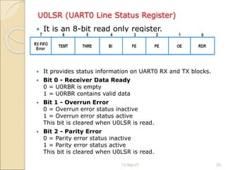
U0LSR (UART0 Line Status Register)
 It is an 8-bit read only register.
 It provides status information on UART0 RX and TX blocks.
 Bit 0 - Receiver Data Ready
0 = U0RBR is empty
1 = U0RBR contains valid data
 Bit 1 - Overrun Error
0 = Overrun error status inactive
1 = Overrun error status active
This bit is cleared when U0LSR is read.
 Bit 2 - Parity Error
0 = Parity error status inactive
1 = Parity error status active
This bit is cleared when U0LSR is read.
13-Sep-21 23
13-Sep-21 24
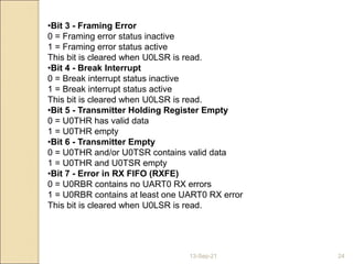
•Bit 3 - Framing Error
0 = Framing error status inactive
1 = Framing error status active
This bit is cleared when U0LSR is read.
•Bit 4 - Break Interrupt
0 = Break interrupt status inactive
1 = Break interrupt status active
This bit is cleared when U0LSR is read.
•Bit 5 - Transmitter Holding Register Empty
0 = U0THR has valid data
1 = U0THR empty
•Bit 6 - Transmitter Empty
0 = U0THR and/or U0TSR contains valid data
1 = U0THR and U0TSR empty
•Bit 7 - Error in RX FIFO (RXFE)
0 = U0RBR contains no UART0 RX errors
1 = U0RBR contains at least one UART0 RX error
This bit is cleared when U0LSR is read.
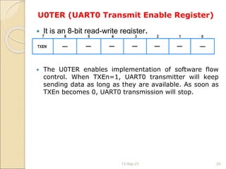
U0TER (UART0 Transmit Enable Register)
 It is an 8-bit read-write register.
 The U0TER enables implementation of software flow
control. When TXEn=1, UART0 transmitter will keep
sending data as long as they are available. As soon as
TXEn becomes 0, UART0 transmission will stop.
13-Sep-21 25
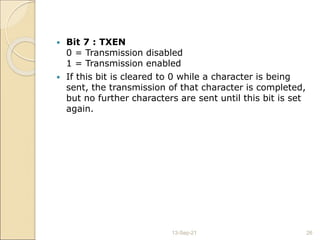
 Bit 7 : TXEN
0 = Transmission disabled
1 = Transmission enabled
 If this bit is cleared to 0 while a character is being
sent, the transmission of that character is completed,
but no further characters are sent until this bit is set
again.
13-Sep-21 26
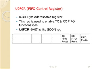
U0FCR (FIFO Control Register)
 8-BIT Byte Addressable register
 This reg is used to enable TX & RX FIFO
functionalities
 U0FCR=0x07 is like SCON reg
13-Sep-21 27
- - - - -
TX
FIFO
Reset
RX
FIFO
Reset
FIFO
Enable
13-Sep-21 28
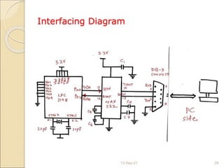
Interfacing Diagram
13-Sep-21 29
Algorithm
13-Sep-21 30
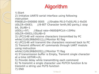
1) Start
2) Initialize UART0 serial interface using following
instruction
PINSEL0=0X0000 0005 ;//Enable P0.0-TxD0,P0.1-RxD0
U0LCR=0X83; //8-BIT Character lenth,NO parity,1 stop
bit, DLAB=1
U0DLL=97; //Baud rate=9600@PCLK=15Mhz
U0LCR=0X03;//DLAB=0
3) LPC2148 will receive characters transmitted by PC
while(!(U0LSR&0X01));//Monitor RI flag
4) LPC2148 will transmit the characters received back to PC
3) Transmit different AT commands through UART module
using instruction
while(!(U0LSR&0X20));//Monitor TI flag
4) If transmission buffer is Empty, Transmit single character
at a time U0THR=ch;
5) Provide delay while transmitting each command
6) To transmit a single character use PUTCH function & to
transmit a string use PUTS function
7) END
13-Sep-21 31
Thankyou

More Related Content

What's hot

PIC Microcontrollers.ppt
PIC Microcontrollers.pptPIC Microcontrollers.ppt
PIC Microcontrollers.ppt
Dr.YNM
 
Memory interfacing
Memory interfacingMemory interfacing
Memory interfacing
mahalakshmimalini
 
Internal architecture-of-8086
Internal architecture-of-8086Internal architecture-of-8086
Internal architecture-of-8086
Estiak Khan
 
8085 microprocessor architecture
8085 microprocessor architecture8085 microprocessor architecture
8085 microprocessor architecture
Arashdeepkaur16
 
Introduction to Arduino Hardware and Programming
Introduction to Arduino Hardware and ProgrammingIntroduction to Arduino Hardware and Programming
Introduction to Arduino Hardware and Programming
Emmanuel Obot
 
Uart
UartUart
I2c protocol - Inter–Integrated Circuit Communication Protocol
I2c protocol - Inter–Integrated Circuit Communication ProtocolI2c protocol - Inter–Integrated Circuit Communication Protocol
I2c protocol - Inter–Integrated Circuit Communication Protocol
Ankur Soni
 
intel 8086 introduction
intel 8086 introductionintel 8086 introduction
intel 8086 introduction
Homoud Alsohaibi
 
SYBSC IT SEM IV EMBEDDED SYSTEMS UNIT I Core of Embedded Systems
SYBSC IT SEM IV EMBEDDED SYSTEMS UNIT I   Core of Embedded SystemsSYBSC IT SEM IV EMBEDDED SYSTEMS UNIT I   Core of Embedded Systems
SYBSC IT SEM IV EMBEDDED SYSTEMS UNIT I Core of Embedded Systems
Arti Parab Academics
 
Introduction to arm processor
Introduction to arm processorIntroduction to arm processor
Introduction to arm processor
RAMPRAKASHT1
 
INTRODUCTION TO MICROCONTROLLER
INTRODUCTION TO MICROCONTROLLERINTRODUCTION TO MICROCONTROLLER
INTRODUCTION TO MICROCONTROLLER
Ankita Jaiswal
 
8259 Programmable Interrupt Controller
8259 Programmable Interrupt Controller8259 Programmable Interrupt Controller
8259 Programmable Interrupt Controller
abhikalmegh
 
LPC 2148 ARM MICROCONTROLLER
LPC 2148 ARM MICROCONTROLLERLPC 2148 ARM MICROCONTROLLER
LPC 2148 ARM MICROCONTROLLER
sravannunna24
 
Introducion to MSP430 Microcontroller.pptx
Introducion to MSP430 Microcontroller.pptxIntroducion to MSP430 Microcontroller.pptx
Introducion to MSP430 Microcontroller.pptx
Dr.YNM
 
ARM Micro-controller
ARM Micro-controllerARM Micro-controller
ARM Micro-controller
Ravikumar Tiwari
 
Interfacing with peripherals: analog to digital converters and digital to ana...
Interfacing with peripherals: analog to digital converters and digital to ana...Interfacing with peripherals: analog to digital converters and digital to ana...
Interfacing with peripherals: analog to digital converters and digital to ana...
NimeshSingh27
 
Architecture of 8086 Microprocessor
Architecture of 8086 Microprocessor  Architecture of 8086 Microprocessor
Architecture of 8086 Microprocessor Mustapha Fatty
 
SPI Protocol
SPI ProtocolSPI Protocol
SPI Protocol
Anurag Tomar
 

What's hot (20)

PIC Microcontrollers.ppt
PIC Microcontrollers.pptPIC Microcontrollers.ppt
PIC Microcontrollers.ppt
 
Memory interfacing
Memory interfacingMemory interfacing
Memory interfacing
 
Internal architecture-of-8086
Internal architecture-of-8086Internal architecture-of-8086
Internal architecture-of-8086
 
8085 microprocessor architecture
8085 microprocessor architecture8085 microprocessor architecture
8085 microprocessor architecture
 
Introduction to Arduino Hardware and Programming
Introduction to Arduino Hardware and ProgrammingIntroduction to Arduino Hardware and Programming
Introduction to Arduino Hardware and Programming
 
Lpc2148 i2c
Lpc2148 i2cLpc2148 i2c
Lpc2148 i2c
 
Uart
UartUart
Uart
 
I2c protocol - Inter–Integrated Circuit Communication Protocol
I2c protocol - Inter–Integrated Circuit Communication ProtocolI2c protocol - Inter–Integrated Circuit Communication Protocol
I2c protocol - Inter–Integrated Circuit Communication Protocol
 
intel 8086 introduction
intel 8086 introductionintel 8086 introduction
intel 8086 introduction
 
SYBSC IT SEM IV EMBEDDED SYSTEMS UNIT I Core of Embedded Systems
SYBSC IT SEM IV EMBEDDED SYSTEMS UNIT I   Core of Embedded SystemsSYBSC IT SEM IV EMBEDDED SYSTEMS UNIT I   Core of Embedded Systems
SYBSC IT SEM IV EMBEDDED SYSTEMS UNIT I Core of Embedded Systems
 
Introduction to arm processor
Introduction to arm processorIntroduction to arm processor
Introduction to arm processor
 
8086 architecture By Er. Swapnil Kaware
8086 architecture By Er. Swapnil Kaware8086 architecture By Er. Swapnil Kaware
8086 architecture By Er. Swapnil Kaware
 
INTRODUCTION TO MICROCONTROLLER
INTRODUCTION TO MICROCONTROLLERINTRODUCTION TO MICROCONTROLLER
INTRODUCTION TO MICROCONTROLLER
 
8259 Programmable Interrupt Controller
8259 Programmable Interrupt Controller8259 Programmable Interrupt Controller
8259 Programmable Interrupt Controller
 
LPC 2148 ARM MICROCONTROLLER
LPC 2148 ARM MICROCONTROLLERLPC 2148 ARM MICROCONTROLLER
LPC 2148 ARM MICROCONTROLLER
 
Introducion to MSP430 Microcontroller.pptx
Introducion to MSP430 Microcontroller.pptxIntroducion to MSP430 Microcontroller.pptx
Introducion to MSP430 Microcontroller.pptx
 
ARM Micro-controller
ARM Micro-controllerARM Micro-controller
ARM Micro-controller
 
Interfacing with peripherals: analog to digital converters and digital to ana...
Interfacing with peripherals: analog to digital converters and digital to ana...Interfacing with peripherals: analog to digital converters and digital to ana...
Interfacing with peripherals: analog to digital converters and digital to ana...
 
Architecture of 8086 Microprocessor
Architecture of 8086 Microprocessor  Architecture of 8086 Microprocessor
Architecture of 8086 Microprocessor
 
SPI Protocol
SPI ProtocolSPI Protocol
SPI Protocol
 

Similar to UART

Llpc2148 sci
Llpc2148 sciLlpc2148 sci
Llpc2148 scianishgoel
 
4 ql uart_psb_ds_revc
4 ql uart_psb_ds_revc4 ql uart_psb_ds_revc
4 ql uart_psb_ds_revc
Doped Maverick
 
Embedded systems, 8051 microcontroller
Embedded systems, 8051 microcontrollerEmbedded systems, 8051 microcontroller
Embedded systems, 8051 microcontrollerAmandeep Alag
 
Registers
RegistersRegisters
Registers
Jamia Hamdard
 
Microprocessor 8051
Microprocessor 8051Microprocessor 8051
Microprocessor 8051Anil Maurya
 
lesson01.ppt
lesson01.pptlesson01.ppt
lesson01.ppt
SushmaHiremath17
 
Presentation On: "Micro-controller 8051 & Embedded System"
Presentation On: "Micro-controller 8051 & Embedded System"Presentation On: "Micro-controller 8051 & Embedded System"
Presentation On: "Micro-controller 8051 & Embedded System"
surabhii007
 
8051 architecture
8051 architecture8051 architecture
8051 architecture
sb108ec
 
AN INTRODUCTION TO SERIAL PORT INTERFACING
AN INTRODUCTION TO SERIAL PORT INTERFACINGAN INTRODUCTION TO SERIAL PORT INTERFACING
AN INTRODUCTION TO SERIAL PORT INTERFACING
Total Project Solutions
 
janakiraman egsp collage I msc 4 unit
janakiraman egsp collage  I msc 4 unitjanakiraman egsp collage  I msc 4 unit
janakiraman egsp collage I msc 4 unit
janakiramang6
 
janakiraman I msc 4 unit
janakiraman I msc 4 unitjanakiraman I msc 4 unit
janakiraman I msc 4 unit
janakiramang6
 
ECE 310 22232 Unit II.pptx
ECE 310 22232 Unit II.pptxECE 310 22232 Unit II.pptx
ECE 310 22232 Unit II.pptx
AkhilNameirakpam
 
moving message display of lcd
 moving message display of lcd moving message display of lcd
moving message display of lcd
abhishek upadhyay
 
8051 Microcontroller Overview by Venkatrao Ramisetti
8051 Microcontroller Overview by Venkatrao Ramisetti 8051 Microcontroller Overview by Venkatrao Ramisetti
8051 Microcontroller Overview by Venkatrao Ramisetti
VenkatraoRamisetti
 
Achieving Reduced Area and Power with Multi Bit Flip-Flop When Implemented In...
Achieving Reduced Area and Power with Multi Bit Flip-Flop When Implemented In...Achieving Reduced Area and Power with Multi Bit Flip-Flop When Implemented In...
Achieving Reduced Area and Power with Multi Bit Flip-Flop When Implemented In...
IJERA Editor
 
Live B tech Projects & Industrial Training @Technogroovy
Live B tech Projects & Industrial Training @Technogroovy Live B tech Projects & Industrial Training @Technogroovy
Live B tech Projects & Industrial Training @Technogroovy
Technogroovy India
 
Microcontroller 8051
Microcontroller 8051Microcontroller 8051
Microcontroller 8051
guest70d48b1
 

Similar to UART (20)

Llpc2148 sci
Llpc2148 sciLlpc2148 sci
Llpc2148 sci
 
4 ql uart_psb_ds_revc
4 ql uart_psb_ds_revc4 ql uart_psb_ds_revc
4 ql uart_psb_ds_revc
 
Embedded systems, 8051 microcontroller
Embedded systems, 8051 microcontrollerEmbedded systems, 8051 microcontroller
Embedded systems, 8051 microcontroller
 
Registers
RegistersRegisters
Registers
 
Microprocessor 8051
Microprocessor 8051Microprocessor 8051
Microprocessor 8051
 
lesson01.ppt
lesson01.pptlesson01.ppt
lesson01.ppt
 
Presentation On: "Micro-controller 8051 & Embedded System"
Presentation On: "Micro-controller 8051 & Embedded System"Presentation On: "Micro-controller 8051 & Embedded System"
Presentation On: "Micro-controller 8051 & Embedded System"
 
8051 architecture
8051 architecture8051 architecture
8051 architecture
 
AN INTRODUCTION TO SERIAL PORT INTERFACING
AN INTRODUCTION TO SERIAL PORT INTERFACINGAN INTRODUCTION TO SERIAL PORT INTERFACING
AN INTRODUCTION TO SERIAL PORT INTERFACING
 
janakiraman egsp collage I msc 4 unit
janakiraman egsp collage  I msc 4 unitjanakiraman egsp collage  I msc 4 unit
janakiraman egsp collage I msc 4 unit
 
UART.pptx
UART.pptxUART.pptx
UART.pptx
 
Project
ProjectProject
Project
 
janakiraman I msc 4 unit
janakiraman I msc 4 unitjanakiraman I msc 4 unit
janakiraman I msc 4 unit
 
ECE 310 22232 Unit II.pptx
ECE 310 22232 Unit II.pptxECE 310 22232 Unit II.pptx
ECE 310 22232 Unit II.pptx
 
231456 006
231456 006231456 006
231456 006
 
moving message display of lcd
 moving message display of lcd moving message display of lcd
moving message display of lcd
 
8051 Microcontroller Overview by Venkatrao Ramisetti
8051 Microcontroller Overview by Venkatrao Ramisetti 8051 Microcontroller Overview by Venkatrao Ramisetti
8051 Microcontroller Overview by Venkatrao Ramisetti
 
Achieving Reduced Area and Power with Multi Bit Flip-Flop When Implemented In...
Achieving Reduced Area and Power with Multi Bit Flip-Flop When Implemented In...Achieving Reduced Area and Power with Multi Bit Flip-Flop When Implemented In...
Achieving Reduced Area and Power with Multi Bit Flip-Flop When Implemented In...
 
Live B tech Projects & Industrial Training @Technogroovy
Live B tech Projects & Industrial Training @Technogroovy Live B tech Projects & Industrial Training @Technogroovy
Live B tech Projects & Industrial Training @Technogroovy
 
Microcontroller 8051
Microcontroller 8051Microcontroller 8051
Microcontroller 8051
 

Recently uploaded

TECHNICAL TRAINING MANUAL GENERAL FAMILIARIZATION COURSE
TECHNICAL TRAINING MANUAL   GENERAL FAMILIARIZATION COURSETECHNICAL TRAINING MANUAL   GENERAL FAMILIARIZATION COURSE
TECHNICAL TRAINING MANUAL GENERAL FAMILIARIZATION COURSE
DuvanRamosGarzon1
 
road safety engineering r s e unit 3.pdf
road safety engineering  r s e unit 3.pdfroad safety engineering  r s e unit 3.pdf
road safety engineering r s e unit 3.pdf
VENKATESHvenky89705
 
Automobile Management System Project Report.pdf
Automobile Management System Project Report.pdfAutomobile Management System Project Report.pdf
Automobile Management System Project Report.pdf
Kamal Acharya
 
addressing modes in computer architecture
addressing modes  in computer architectureaddressing modes  in computer architecture
addressing modes in computer architecture
ShahidSultan24
 
Planning Of Procurement o different goods and services
Planning Of Procurement o different goods and servicesPlanning Of Procurement o different goods and services
Planning Of Procurement o different goods and services
JoytuBarua2
 
DESIGN A COTTON SEED SEPARATION MACHINE.docx
DESIGN A COTTON SEED SEPARATION MACHINE.docxDESIGN A COTTON SEED SEPARATION MACHINE.docx
DESIGN A COTTON SEED SEPARATION MACHINE.docx
FluxPrime1
 
CME397 Surface Engineering- Professional Elective
CME397 Surface Engineering- Professional ElectiveCME397 Surface Engineering- Professional Elective
CME397 Surface Engineering- Professional Elective
karthi keyan
 
Standard Reomte Control Interface - Neometrix
Standard Reomte Control Interface - NeometrixStandard Reomte Control Interface - Neometrix
Standard Reomte Control Interface - Neometrix
Neometrix_Engineering_Pvt_Ltd
 
LIGA(E)11111111111111111111111111111111111111111.ppt
LIGA(E)11111111111111111111111111111111111111111.pptLIGA(E)11111111111111111111111111111111111111111.ppt
LIGA(E)11111111111111111111111111111111111111111.ppt
ssuser9bd3ba
 
HYDROPOWER - Hydroelectric power generation
HYDROPOWER - Hydroelectric power generationHYDROPOWER - Hydroelectric power generation
HYDROPOWER - Hydroelectric power generation
Robbie Edward Sayers
 
power quality voltage fluctuation UNIT - I.pptx
power quality voltage fluctuation UNIT - I.pptxpower quality voltage fluctuation UNIT - I.pptx
power quality voltage fluctuation UNIT - I.pptx
ViniHema
 
The role of big data in decision making.
The role of big data in decision making.The role of big data in decision making.
The role of big data in decision making.
ankuprajapati0525
 
Halogenation process of chemical process industries
Halogenation process of chemical process industriesHalogenation process of chemical process industries
Halogenation process of chemical process industries
MuhammadTufail242431
 
Courier management system project report.pdf
Courier management system project report.pdfCourier management system project report.pdf
Courier management system project report.pdf
Kamal Acharya
 
J.Yang, ICLR 2024, MLILAB, KAIST AI.pdf
J.Yang,  ICLR 2024, MLILAB, KAIST AI.pdfJ.Yang,  ICLR 2024, MLILAB, KAIST AI.pdf
J.Yang, ICLR 2024, MLILAB, KAIST AI.pdf
MLILAB
 
在线办理(ANU毕业证书)澳洲国立大学毕业证录取通知书一模一样
在线办理(ANU毕业证书)澳洲国立大学毕业证录取通知书一模一样在线办理(ANU毕业证书)澳洲国立大学毕业证录取通知书一模一样
在线办理(ANU毕业证书)澳洲国立大学毕业证录取通知书一模一样
obonagu
 
Event Management System Vb Net Project Report.pdf
Event Management System Vb Net  Project Report.pdfEvent Management System Vb Net  Project Report.pdf
Event Management System Vb Net Project Report.pdf
Kamal Acharya
 
The Benefits and Techniques of Trenchless Pipe Repair.pdf
The Benefits and Techniques of Trenchless Pipe Repair.pdfThe Benefits and Techniques of Trenchless Pipe Repair.pdf
The Benefits and Techniques of Trenchless Pipe Repair.pdf
Pipe Restoration Solutions
 
Cosmetic shop management system project report.pdf
Cosmetic shop management system project report.pdfCosmetic shop management system project report.pdf
Cosmetic shop management system project report.pdf
Kamal Acharya
 
Democratizing Fuzzing at Scale by Abhishek Arya
Democratizing Fuzzing at Scale by Abhishek AryaDemocratizing Fuzzing at Scale by Abhishek Arya
Democratizing Fuzzing at Scale by Abhishek Arya
abh.arya
 

Recently uploaded (20)

TECHNICAL TRAINING MANUAL GENERAL FAMILIARIZATION COURSE
TECHNICAL TRAINING MANUAL   GENERAL FAMILIARIZATION COURSETECHNICAL TRAINING MANUAL   GENERAL FAMILIARIZATION COURSE
TECHNICAL TRAINING MANUAL GENERAL FAMILIARIZATION COURSE
 
road safety engineering r s e unit 3.pdf
road safety engineering  r s e unit 3.pdfroad safety engineering  r s e unit 3.pdf
road safety engineering r s e unit 3.pdf
 
Automobile Management System Project Report.pdf
Automobile Management System Project Report.pdfAutomobile Management System Project Report.pdf
Automobile Management System Project Report.pdf
 
addressing modes in computer architecture
addressing modes  in computer architectureaddressing modes  in computer architecture
addressing modes in computer architecture
 
Planning Of Procurement o different goods and services
Planning Of Procurement o different goods and servicesPlanning Of Procurement o different goods and services
Planning Of Procurement o different goods and services
 
DESIGN A COTTON SEED SEPARATION MACHINE.docx
DESIGN A COTTON SEED SEPARATION MACHINE.docxDESIGN A COTTON SEED SEPARATION MACHINE.docx
DESIGN A COTTON SEED SEPARATION MACHINE.docx
 
CME397 Surface Engineering- Professional Elective
CME397 Surface Engineering- Professional ElectiveCME397 Surface Engineering- Professional Elective
CME397 Surface Engineering- Professional Elective
 
Standard Reomte Control Interface - Neometrix
Standard Reomte Control Interface - NeometrixStandard Reomte Control Interface - Neometrix
Standard Reomte Control Interface - Neometrix
 
LIGA(E)11111111111111111111111111111111111111111.ppt
LIGA(E)11111111111111111111111111111111111111111.pptLIGA(E)11111111111111111111111111111111111111111.ppt
LIGA(E)11111111111111111111111111111111111111111.ppt
 
HYDROPOWER - Hydroelectric power generation
HYDROPOWER - Hydroelectric power generationHYDROPOWER - Hydroelectric power generation
HYDROPOWER - Hydroelectric power generation
 
power quality voltage fluctuation UNIT - I.pptx
power quality voltage fluctuation UNIT - I.pptxpower quality voltage fluctuation UNIT - I.pptx
power quality voltage fluctuation UNIT - I.pptx
 
The role of big data in decision making.
The role of big data in decision making.The role of big data in decision making.
The role of big data in decision making.
 
Halogenation process of chemical process industries
Halogenation process of chemical process industriesHalogenation process of chemical process industries
Halogenation process of chemical process industries
 
Courier management system project report.pdf
Courier management system project report.pdfCourier management system project report.pdf
Courier management system project report.pdf
 
J.Yang, ICLR 2024, MLILAB, KAIST AI.pdf
J.Yang,  ICLR 2024, MLILAB, KAIST AI.pdfJ.Yang,  ICLR 2024, MLILAB, KAIST AI.pdf
J.Yang, ICLR 2024, MLILAB, KAIST AI.pdf
 
在线办理(ANU毕业证书)澳洲国立大学毕业证录取通知书一模一样
在线办理(ANU毕业证书)澳洲国立大学毕业证录取通知书一模一样在线办理(ANU毕业证书)澳洲国立大学毕业证录取通知书一模一样
在线办理(ANU毕业证书)澳洲国立大学毕业证录取通知书一模一样
 
Event Management System Vb Net Project Report.pdf
Event Management System Vb Net  Project Report.pdfEvent Management System Vb Net  Project Report.pdf
Event Management System Vb Net Project Report.pdf
 
The Benefits and Techniques of Trenchless Pipe Repair.pdf
The Benefits and Techniques of Trenchless Pipe Repair.pdfThe Benefits and Techniques of Trenchless Pipe Repair.pdf
The Benefits and Techniques of Trenchless Pipe Repair.pdf
 
Cosmetic shop management system project report.pdf
Cosmetic shop management system project report.pdfCosmetic shop management system project report.pdf
Cosmetic shop management system project report.pdf
 
Democratizing Fuzzing at Scale by Abhishek Arya
Democratizing Fuzzing at Scale by Abhishek AryaDemocratizing Fuzzing at Scale by Abhishek Arya
Democratizing Fuzzing at Scale by Abhishek Arya
 

UART

  • 1. Name of Subject Advanced Processor Subject code 304189 Year 2020-21 Class TE E&Tc Semester VI Examination Scheme In-Sem(Paper)-30 Marks End-Sem(Paper)-70 Marks Unit no III Name of Unit Real World Interfacing with ARM7 Based Microcontroller-1 13-Sep-21 1
  • 2. 13-Sep-21 2 Course Objectives CO1 To understand need and application of ARM Microprocessors in embedded system. CO2 To study the architecture of ARM series microprocessor CO3 To understand architecture and features of typical ARM7& DSP Processors. CO4 To learn interfacing of real world input and output devices CO5 To learn embedded communication systems.
  • 3. 13-Sep-21 3 Course Outcomes CO1 Describe the ARM microprocessor architectures and its features. CO2 Design embedded system with available resources. CO3 Interface the advanced peripherals to ARM based microcontroller CO4 Use of DSP Processors and resources for signal processing applications
  • 5. UART(Universal Asynchronous Receiver/Transmitter) 13-Sep-21 5  It is a serial communication protocol in which data is transferred serially bit by bit at a time.  Asynchronous serial communication is widely used for byte oriented transmission.  In Asynchronous serial communication, a byte of data is transferred at a time.  UART serial communication protocol uses a defined frame structure for their data bytes. Frame structure in Asynchronous communication consists :  START bit: It is a bit with which indicates that serial communication has started and it is always low.  Data bits packet: Data bits can be packets of 5 to 9 bits. Normally we use 8 bit data packet, which is always sent after the START bit.  STOP bit: This usually is one or two bits in length. It is sent after data bits packet to indicate the end of frame. Stop bit is always logic high.
  • 7. UART module  LPC2148 has 2-UARTs numbering 0-1, similarly, the pins are also named as RXD0-RXD1 and TXD0-TXD1  As the LPC2148 pins are multiplexed for multiple functionalities, first they have to be configured as UART pins.  Below table shows the multiplexed UART's pins. 13-Sep-21 7 Port Pin Pin Number PINSEL_FUNC_0 PINSEL_FUNC_1 PINSEL_FUNC_2 PINSEL_FUNC_3 P0.0 19 GPIO TXD0 PWM1 P0.1 21 GPIO RXD0 PWM3 EINT0 P0_8 33 GPIO TXD1 PWM4 AD1.1 P0.9 34 GPIO RXD1 PWM6 EINT3
  • 8. PINSEL 0 31……0 Bit Symbol Value Function 1:0 P0.0 00 GPIO port 0.0 01 TXD(UART 0) 10 PWM1 11 RESERVED 3:2 P0.1 00 GPIO P0.1 01 RXD(UART0) 10 PWM3 11 EINT0 13-Sep-21 8
  • 9. Features  UART0  16 byte Receive and Transmit FIFOs  Built-in fractional baud rate generator with autobauding capabilities  Software flow control through TXEN bit in Transmit Enable Register  UART1  16 byte Receive and Transmit FIFOs  Built-in fractional baud rate generator with autobauding capabilities  Software and hardware flow control implementation possible  Standard modem interface signals included with flow control fully supported in hardware 13-Sep-21 9
  • 10. Register Description UxRBR Contains the recently received Data UxTHR Contains the data to be transmitted UxFCR FIFO Control Register UxLCR Controls the UART frame formatting(Number of Data Bits, Stop bits) UxDLL Least Significant Byte of the UART baud rate generator value. UxDLM Most Significant Byte of the UART baud rate generator value. 13-Sep-21 10 UART Registers
  • 12. UART0 Registers U0RBR (UART0 Receive Buffer Register)  It is an 8-bit read only register.  This register contains the received data.  It contains the “oldest” received byte in the receive FIFO.  If the character received is less than 8 bits, the unused MSBs are padded with zeroes.  The Divisor Latch Access Bit (DLAB) in U0LCR must be zero in order to access the U0RBR. (DLAB = 0) 13-Sep-21 12
  • 13. U0THR (UART0 Transmit Holding Register)  It is an 8-bit write only register.  Data to be transmitted is written to this register.  It contains the “newest” received byte in the transmit FIFO.  The Divisor Latch Access Bit (DLAB) in U0LCR must be zero in order to access theU0THR. (DLAB = 0) 13-Sep-21 13
  • 14. U0DLL and U0DLM (UART0 Divisor Latch Registers)  Both of them hold 8-bit values.  These register together form a 16 bit divisor value which is used in baud rate generation.  U0DLM holds the upper 8 bits and U0DLL holds the lower 8 bits and the formation is “[U0DLM:U0DLL].  Since these form a divisor value and division by zero is invalid,the starting for U0DLL is 0x01(not 0x00)i.e starting value in combined formation is[0x00:0x01] i.e.0x0001.  In order to access and use these registers properly,DLAB bit in U0LCR must be set to 1. 13-Sep-21 14
  • 15. U0FDR (UART0 Fractional Divider Register) • It is a 32-bit read write register. • It decides the clock pre-scalar for baud rate generation. • If fractional divider is active (i.e. DIVADDVAL>0) and DLM = 0, DLL must be greater than 3.  If DIVADDVAL is 0, the fractional baud rate generator will not impact the UART0 baud rate.  Reset value of DIVADDVAL is 0.  MULVAL must be greater than or equal to 1 for UART0 to operate properly, regardless of whether the fractional baud rate generator is used or not.  Reset value of MULVAL is 1. 13-Sep-21 15
  • 16.  The formula for UART0 baud rate is given below  MULVAL and DIVADDVAL should have values in the range of 0 to 15. If this is not ensured, the output of the fractional divider is undefined.  The value of the U0FDR should not be modified while transmitting/receiving data.  This may result in corruption of data. 13-Sep-21 16
  • 17. U0IER (UART0 Interrupt Enable Register)  It is a 32-bit read-write register.  It is used to enable UART0 interrupt sources.  DLAB should be zero (DLAB = 0).  Bit 0 - RBR Interrupt Enable. It also controls the Character Receive Time-Out interrupt. 0 = Disable Receive Data Available interrupt 1 = Enable Receive Data Available interrupt  Bit 1 - THRE Interrupt Enable 0 = Disable THRE interrupt 1 = Enable THRE interrupt  Bit 2 - RX Line Interrupt Enable 0 = Disable UART0 RX line status interrupts 1 = EnableUART0 RX line status interrupts 13-Sep-21 17
  • 18.  Bit 8 - ABEO Interrupt Enable 0 = Disable auto-baud time-out interrupt 1 = Enable auto-baud time-out interrupt  Bit 9 - ABTO Interrupt Enable 0 = Disable end of auto-baud interrupt 1 = Enable the end of auto-baud interrupt 13-Sep-21 18
  • 19. U0LCR (UART0 Line Control Register)  It is an 8-bit read-write register.  It determines the format of the data character that is to be transmitted or received 13-Sep-21 19
  • 20. 13-Sep-21 20 •Bit 1:0 - Word Length Select 00 = 5-bit character length 01 = 6-bit character length 10 = 7-bit character length 11 = 8-bit character length •Bit 2 - Number of Stop Bits 0 = 1 stop bit 1 = 2 stop bits •Bit 3 - Parity Enable 0 = Disable parity generation and checking 1 = Enable parity generation and checking •Bit 5:4 - Parity Select 00 = Odd Parity 01 = Even Parity 10 = Forced “1” Stick Parity 11 = Forced “0” Stick Parity •Bit 6 - Break Control 0= Disable break transmission 1 = Enable break transmission •Bit 7 - Divisor Latch Access Bit (DLAB) 0 = Disable access to Divisor Latches 1 = Enable access to Divisor Latches
  • 21. U0IIR (UART0 Interrupt Identification Register)  It is a 32-bit read only register.  It provides a status code that denotes the  It provides a status code that denotes the priority and source of a pending interrupt.  It must be read before executing the Interrupt Service Routine to clear the interrupt.  Bit 0 - Interrupt Pending 0 = At least one interrupt is pending 1 = No interrupts pending  Bit 3:1 - Interrupt Identification Identifies an interrupt corresponding to theUART0 Rx FIFO. 011 = Receive Line Status (RLS) Interrupt 010 = Receive Data Available (RDA) Interrupt 13-Sep-21 21
  • 22.  Bit 7:6 - FIFO Enable These bits are equivalent to FIFO enable bit in FIFO Control Register, 0 = If FIFOs are disabled 1 = FIFOs are enabled  Bit 8 - ABEO Interrupt(End of Auto-Baud ) If interrupt is enabled, 0 = No ABEO interrupt 1 = Auto-baud has finished successfully  Bit 9 - ABTO Interrupt (Auto-Baud Time-Out) If interrupt is enabled, 0 = No ABTO interrupt 1 = Auto-baud has timed out 13-Sep-21 22
  • 23. U0LSR (UART0 Line Status Register)  It is an 8-bit read only register.  It provides status information on UART0 RX and TX blocks.  Bit 0 - Receiver Data Ready 0 = U0RBR is empty 1 = U0RBR contains valid data  Bit 1 - Overrun Error 0 = Overrun error status inactive 1 = Overrun error status active This bit is cleared when U0LSR is read.  Bit 2 - Parity Error 0 = Parity error status inactive 1 = Parity error status active This bit is cleared when U0LSR is read. 13-Sep-21 23
  • 24. 13-Sep-21 24 •Bit 3 - Framing Error 0 = Framing error status inactive 1 = Framing error status active This bit is cleared when U0LSR is read. •Bit 4 - Break Interrupt 0 = Break interrupt status inactive 1 = Break interrupt status active This bit is cleared when U0LSR is read. •Bit 5 - Transmitter Holding Register Empty 0 = U0THR has valid data 1 = U0THR empty •Bit 6 - Transmitter Empty 0 = U0THR and/or U0TSR contains valid data 1 = U0THR and U0TSR empty •Bit 7 - Error in RX FIFO (RXFE) 0 = U0RBR contains no UART0 RX errors 1 = U0RBR contains at least one UART0 RX error This bit is cleared when U0LSR is read.
  • 25. U0TER (UART0 Transmit Enable Register)  It is an 8-bit read-write register.  The U0TER enables implementation of software flow control. When TXEn=1, UART0 transmitter will keep sending data as long as they are available. As soon as TXEn becomes 0, UART0 transmission will stop. 13-Sep-21 25
  • 26.  Bit 7 : TXEN 0 = Transmission disabled 1 = Transmission enabled  If this bit is cleared to 0 while a character is being sent, the transmission of that character is completed, but no further characters are sent until this bit is set again. 13-Sep-21 26
  • 27. U0FCR (FIFO Control Register)  8-BIT Byte Addressable register  This reg is used to enable TX & RX FIFO functionalities  U0FCR=0x07 is like SCON reg 13-Sep-21 27 - - - - - TX FIFO Reset RX FIFO Reset FIFO Enable
  • 30. Algorithm 13-Sep-21 30 1) Start 2) Initialize UART0 serial interface using following instruction PINSEL0=0X0000 0005 ;//Enable P0.0-TxD0,P0.1-RxD0 U0LCR=0X83; //8-BIT Character lenth,NO parity,1 stop bit, DLAB=1 U0DLL=97; //Baud rate=9600@PCLK=15Mhz U0LCR=0X03;//DLAB=0 3) LPC2148 will receive characters transmitted by PC while(!(U0LSR&0X01));//Monitor RI flag 4) LPC2148 will transmit the characters received back to PC 3) Transmit different AT commands through UART module using instruction while(!(U0LSR&0X20));//Monitor TI flag 4) If transmission buffer is Empty, Transmit single character at a time U0THR=ch; 5) Provide delay while transmitting each command 6) To transmit a single character use PUTCH function & to transmit a string use PUTS function 7) END