Download to read offline
![DS748 July 25, 2012 www.xilinx.com 5
Product Specification
LogiCORE IP AXI UART 16550 (v1.01a)
I/O Signals
The I/O signals are listed and described in Table 1.
Table 1: I/O Signals
Port Signal Name Interface I/O
Initial
State
Description
System Signals
P1 S_AXI_ACLK System I - AXI Clock
P2 S_AXI_ARESETN System I - AXI Reset signal, active-Low
P3 IP2INTC_Irpt System O 0
Device interrupt output to microprocessor interrupt input
or system interrupt controller (active-High)
P4 Freeze System I - Freezes UART for software debug (active-High)
AXI Write Address Channel Signals
P5
S_AXI_AWADDR[C_S_AXI_
ADDR_WIDTH-1:0]
AXI I -
AXI Write address. The write address bus gives the
address of the write transaction.
P6 S_AXI_AWVALID AXI I -
Write address valid. This signal indicates that valid write
address is available.
P7 S_AXI_AWREADY AXI O 0
Write address ready. This signal indicates that the slave
is ready to accept an address.
AXI Write Channel Signals
P8
S_AXI_WDATA[C_S_AXI_
DATA_WIDTH - 1: 0]
AXI I - Write data
P9
S_AXI_WSTB[C_S_AXI_
DATA_WIDTH/8-1:0] (1) AXI I -
Write strobes. This signal indicates which byte lanes to
update in memory.
P10 S_AXI_WVALID AXI I -
Write valid. This signal indicates that valid write data and
strobes are available.
P11 S_AXI_WREADY AXI O 0
Write ready. This signal indicates that the slave can
accept the write data.
AXI Write Response Channel Signals
P12 S_AXI_BRESP[1:0](2) AXI O 0
Write response. This signal indicates the status of the
write transaction.
“00“ - OKAY
“10“ - SLVERR
P13 S_AXI_BVALID AXI O 0
Write response valid. This signal indicates that a valid
write response is available.
P14 S_AXI_BREADY AXI I -
Response ready. This signal indicates that the master
can accept the response information.
AXI Read Address Channel Signals
P15
S_AXI_ARADDR[C_S_AXI_
ADDR_WIDTH -1:0]
AXI I -
Read address. The read address bus gives the address
of a read transaction.
P16 S_AXI_ARVALID AXI I -
Read address valid. When High, this signal indicates that
the read address is valid and remains stable until the
address acknowledgement signal, S_AXI_ARREADY, is
High.
P17 S_AXI_ARREADY AXI O 1
Read address ready. This signal indicates that the slave
is ready to accept an address.](https://image.slidesharecdn.com/xilinxaxiuart16550-151122021538-lva1-app6892/75/Xilinxaxi-uart16550-5-2048.jpg)
![DS748 July 25, 2012 www.xilinx.com 6
Product Specification
LogiCORE IP AXI UART 16550 (v1.01a)
AXI Read Data Channel Signals
P18
S_AXI_RDATA[C_S_AXI_
DATA_WIDTH -1:0]
AXI O 0 Read data
P19 S_AXI_RRESP[1:0](2) AXI O 0
Read response. This signal indicates the status of the
read transfer.
“00“ - OKAY
“10“ - SLVERR
P20 S_AXI_RVALID AXI O 0
Read valid. This signal indicates that the required read
data is available and the read transfer can complete
P21 S_AXI_RREADY AXI I -
Read ready. This signal indicates that the master can
accept the read data and response information
UART Interface Signals
P22 BaudoutN Serial O 1 16 x clock signal from the transmitter section of the UART
P23 Rclk Serial I -
Receiver 16x clock (Optional, can be driven externally
under control of the C_HAS_EXTERNAL_RCLK
parameter)
P24 Sin Serial I - Serial data input
P25 Sout Serial O 1 Serial data output
P26 Xin Serial I -
Baud rate generator reference clock (Optional, can be
driven externally under control of the
C_HAS_EXTERNAL_XIN parameter)
P27 Xout Serial O 0
If C_HAS_EXTERNAL_XIN = 0, Xout is 0, if
C_HAS_EXTERNAL_XIN = 1 Xout can be used as
reference feedback clock for Baud rate generator
P28 CtsN Modem I -
Clear to send (active-Low).
When Low, this indicates that the MODEM or data set is
ready to exchange data.
P29 DcdN Modem I -
Data carrier detect (active-Low).
When Low, indicates that the data carrier has been
detected by the MODEM or data set.
P30 DsrN Modem I -
Data set ready (active-Low).
When Low, this indicates that the MODEM or data set is
ready to establish the communication link with the UART.
P31 DtrN Modem O 1
Data terminal ready (active-Low).
When Low, this informs the MODEM or data set that the
UART is ready to establish a communication link.
P32 RiN Modem I -
Ring indicator (active-Low).
When Low, this indicates that a telephone ringing signal
has been received by the MODEM or data set.
P33 RtsN Modem O 1
Request to send (active-Low).
When Low, this informs the MODEM or data set that the
UART is ready to exchange data.
P34 Ddis User O 1
Driver disable. This goes Low when CPU is reading data
from UART.
P35 Out1N User O 1 User controlled output
P36 Our2N User O 1 User controlled output
Table 1: I/O Signals (Cont’d)
Port Signal Name Interface I/O
Initial
State
Description](https://image.slidesharecdn.com/xilinxaxiuart16550-151122021538-lva1-app6892/75/Xilinxaxi-uart16550-6-2048.jpg)
![DS748 July 25, 2012 www.xilinx.com 8
Product Specification
LogiCORE IP AXI UART 16550 (v1.01a)
Parameter - Port Dependencies
The dependencies between the AXI UART 16550 core design parameters and I/O signals are described in Table 3.
In addition, when certain features are parameterized out of the design, the related logic is no longer a part of the
design. The unused input signals and related output signals are set to a specified value.
G8
External xin clock
frequency in Hz.
C_EXTERNAL_XIN_CLK_HZ(3) Valid xin clock
frequency in Hz.
25000000 integer
Notes:
1. When C_HAS_EXTERNAL_XIN=0, this core uses S_AXI_ACLK as a reference clock for the baud calculation. User must use
S_AXI_ACLK frequency to calculate baud divisor value for DLL and DLM register configuration.
2. The external xin input clock must be less than half of S_AXI_ACLK.
3. External xin clock frequency. User must configure this parameter when external xin is used. (C_HAS_EXTERNAL_XIN is ‘1’).
Table 3: Parameter-Port Dependencies
Generic
or Port
Name Affects Depends Relationship Description
Design Parameters
G3 C_S_AXI_ADDR_WIDTH P5, P15 - Defines the width of the ports
G4 C_S_AXI_DATA_WIDTH
P8, P9,
P18
- Defines the width of the ports
I/O Signals
P5
S_AXI_AWADDR[C_S_AXI_
ADDR_WIDTH-1:0]
- G3
Port width depends on the generic
C_S_AXI_ADDR_WIDTH
P8
S_AXI_WDATA[C_S_AXI_DATA_W
IDTH-1:0]
- G4
Port width depends on the generic
C_S_AXI_DATA_WIDTH
P9
S_AXI_WSTB[C_S_AXI_DATA_
WIDTH/8-1:0]
- G4
Port width depends on the generic
C_S_AXI_DATA_WIDTH
P15
S_AXI_ARADDR[C_S_AXI_
ADDR_WIDTH -1:0]
- G3
Port width depends on the generic
C_S_AXI_ADDR_WIDTH
P18
S_AXI_RDATA[C_S_AXI_DATA_
WIDTH -1:0]
- G4
Port width depends on the generic
C_S_AXI_DATA_WIDTH
P23 Rclk - G6
If C_HAS_EXTERNAL_RCLK = 0 baudoutN is
used as 16x receiver clock,
C_HAS_EXTERNAL_RCLK = 1, rclk is used as
16x receiver clock.
P26 Xin - G5
When C_HAS_EXTERNAL_XIN = 0, xin is
unconnected, C_HAS_EXTERNAL_XIN = 1, xin is
driven externally.
Table 2: Design Parameters (Cont’d)
Generic Parameter Description Parameter Name Allowable Values Default Value
VHDL
Type](https://image.slidesharecdn.com/xilinxaxiuart16550-151122021538-lva1-app6892/75/Xilinxaxi-uart16550-8-2048.jpg)

![DS748 July 25, 2012 www.xilinx.com 18
Product Specification
LogiCORE IP AXI UART 16550 (v1.01a)
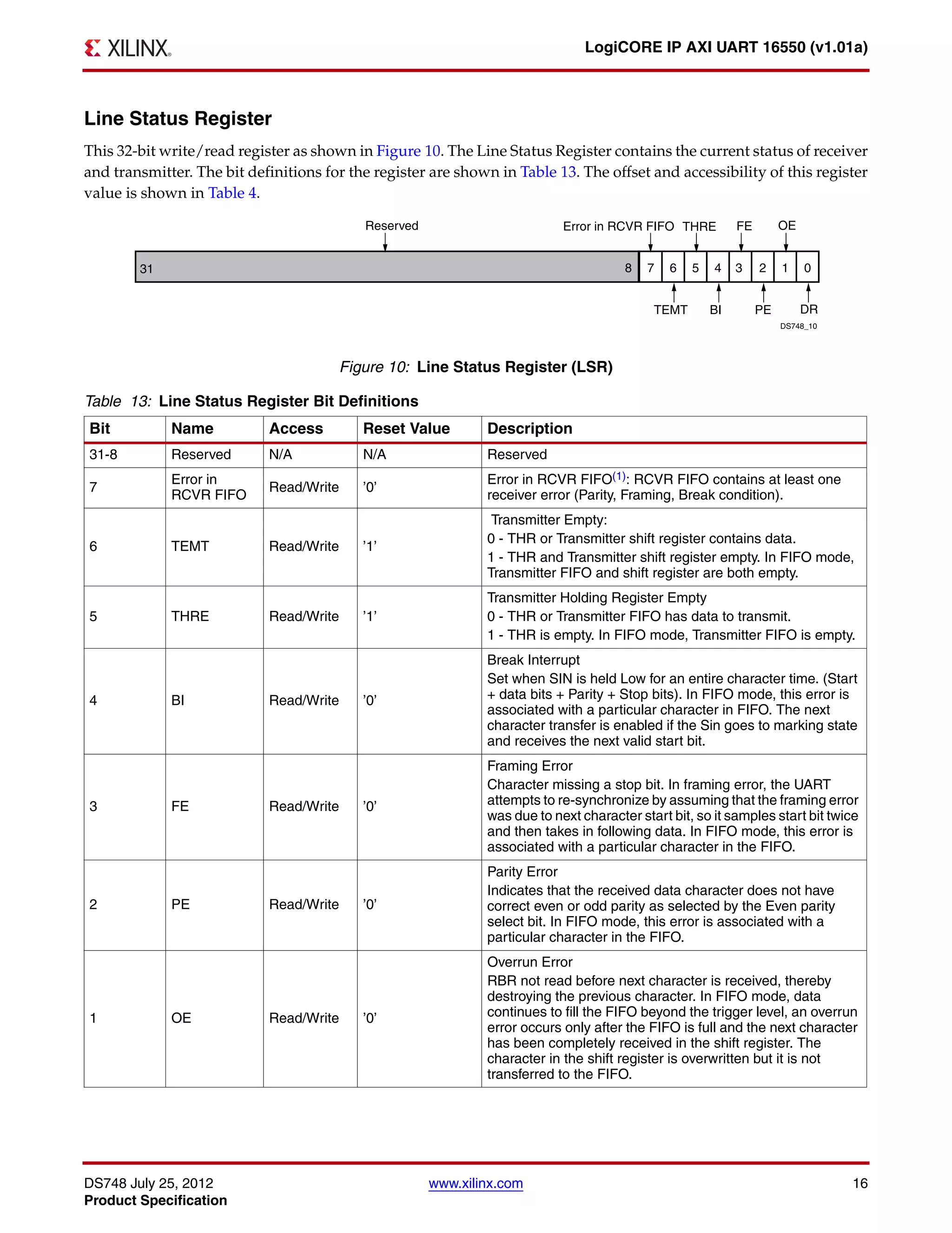
Scratch Register
This 32-bit write/read register is shown in Figure 12. The Scratch Register can be used to hold user data. The bit
definitions for the register are shown in Table 15. The offset and accessibility of this register value is shown in
Table 4.
Divisor Latch (Least Significant Byte) Register
This 32-bit write/read register is shown in Figure 13. The Divisor Latch (Least Significant Byte) Register holds the
least significant byte of the baud rate generator counter. The bit definitions for the register are shown in Table 16.
The offset and accessibility of this register value is shown in Table 4.
X-Ref Target - Figure 12
Figure 12: Scratch Register (SCR)
Table 15: Scratch Register Bit Definitions
Bit Name Access Reset Value Description
31-8 Reserved N/A N/A Reserved.
7-0 Scratch Read/Write "00000000" Hold the data temporarily.
X-Ref Target - Figure 13
Figure 13: Divisor Latch (Least Significant Byte) Register
Table 16: Divisor Latch (Least Significant Byte) Register Bit Definitions
Bit Name Access Reset Value Description
31-8 Reserved N/A N/A Reserved
7-0 DLL Read/Write "XXXXXXXX"(1) Divisor Latch Least Significant Byte
Notes:
1. On reset, the DLL gets configured for 9600 baud. The DLL reset value, [LSB(divisor)] is calculated from the formula, divisor =
C_S_AXI_ACLK_FREQ/(16 x 9600)).](https://image.slidesharecdn.com/xilinxaxiuart16550-151122021538-lva1-app6892/75/Xilinxaxi-uart16550-18-2048.jpg)
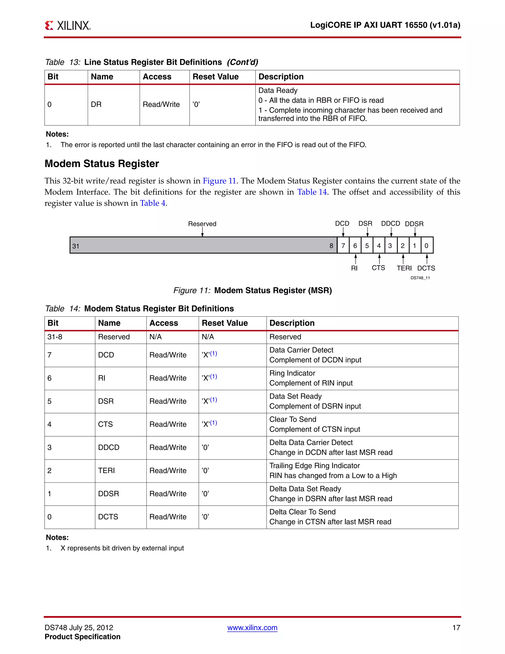
![DS748 July 25, 2012 www.xilinx.com 19
Product Specification
LogiCORE IP AXI UART 16550 (v1.01a)
Divisor Latch (Most Significant Byte) Register
This 32-bit write/read register is shown in Figure 14. The Divisor Latch (Most Significant Byte) Register holds the
most significant byte of the baud rate generator counter. The bit definitions for the register are shown in Table 17.
The offset and accessibility of this register value is shown in Table 4.
User Application Hints
The use of the AXI UART 16550 in 16550 mode is outlined in these steps:
1. The system programmer specifies the format of the asynchronous data communications exchange: for example,
Data bits (5,6,7 or 8), setting of parity ON and selecting on the even or odd parity, setting of the number stop bits
for the transmission, and set the Divisor latch access bit by programming the Line Control Register.
2. Write Interrupt Enable Register to activate the individual interrupts
3. Write to the FIFO Control Register to enable the FIFO’s, clear the FIFO’s, and set the RCVR FIFO trigger level.
4. Write to Divisor Latch least significant byte first, then the Divisor Latch most significant byte second for proper
setting of the baud rate of the UART.
5. Service the interrupts whenever an interrupt is triggered by the AXI UART 16550.
Example 1
An example use of the AXI UART 16550 with the operating mode set to the following parameters in 16550 mode is
outlined in the subsequent numbered steps.
• Baud rate: 56Kbps
• System clock: 100 Mhz (C_HAS_EXTERNAL_XIN = 0)
• Enabled and Threshold settings for the FIFO receive buffer.
• Format of asynchronous data exchange 8 data bits, Even parity and 2 stop bits
1. Write 0x0000_0080 to Line Control Register. This configures the DLAB bit, which allows the writing into the
Divisor Latch’s Least significant and Most significant bytes.
2. Write 0x0000_006F to Divisor Latch’s Least significant byte and write 0x0000_0000 to Divisor Latch’s Most
significant byte in that order. This configures the baud rate setup of UART to 56Kbps operation. The divisor
value is calculated by using following formula:
divisor = (C_S_AXI_ACLK_FREQ/(16 Baud Rate))
X-Ref Target - Figure 14
Figure 14: Divisor Latch (Most Significant Byte) Register
Table 17: Divisor (Most Significant Byte) Register Bit Definitions
Bit Name Access Reset Value Description
31-8 Reserved N/A N/A Reserved
7-0 DLM Read/Write "XXXXXXXX" (1) Divisor Latch Most Significant Byte
Notes:
1. On reset, the DLM gets configured for 9600 baud. The DLM reset value, [MSB(divisor)] is calculated from the formula, divisor =
(C_S_AXI_ACLK_FREQ/(16 x 9600)).
×](https://image.slidesharecdn.com/xilinxaxiuart16550-151122021538-lva1-app6892/75/Xilinxaxi-uart16550-19-2048.jpg)


The document describes the LogiCORE IP AXI UART 16550 core, which provides an AXI interface to a UART 16550 controller. It connects to the AXI bus and provides an interface for asynchronous serial data transfer. Key features include support for standard UART protocols, interrupts, FIFOs, and an AXI4-Lite interface. The core functionality and parameters are described.


![Communication_Protocols[2][1].pptx on protocoals](https://cdn.slidesharecdn.com/ss_thumbnails/communicationprotocols21-250429164707-38355411-thumbnail.jpg?width=640&height=640&fit=bounds)