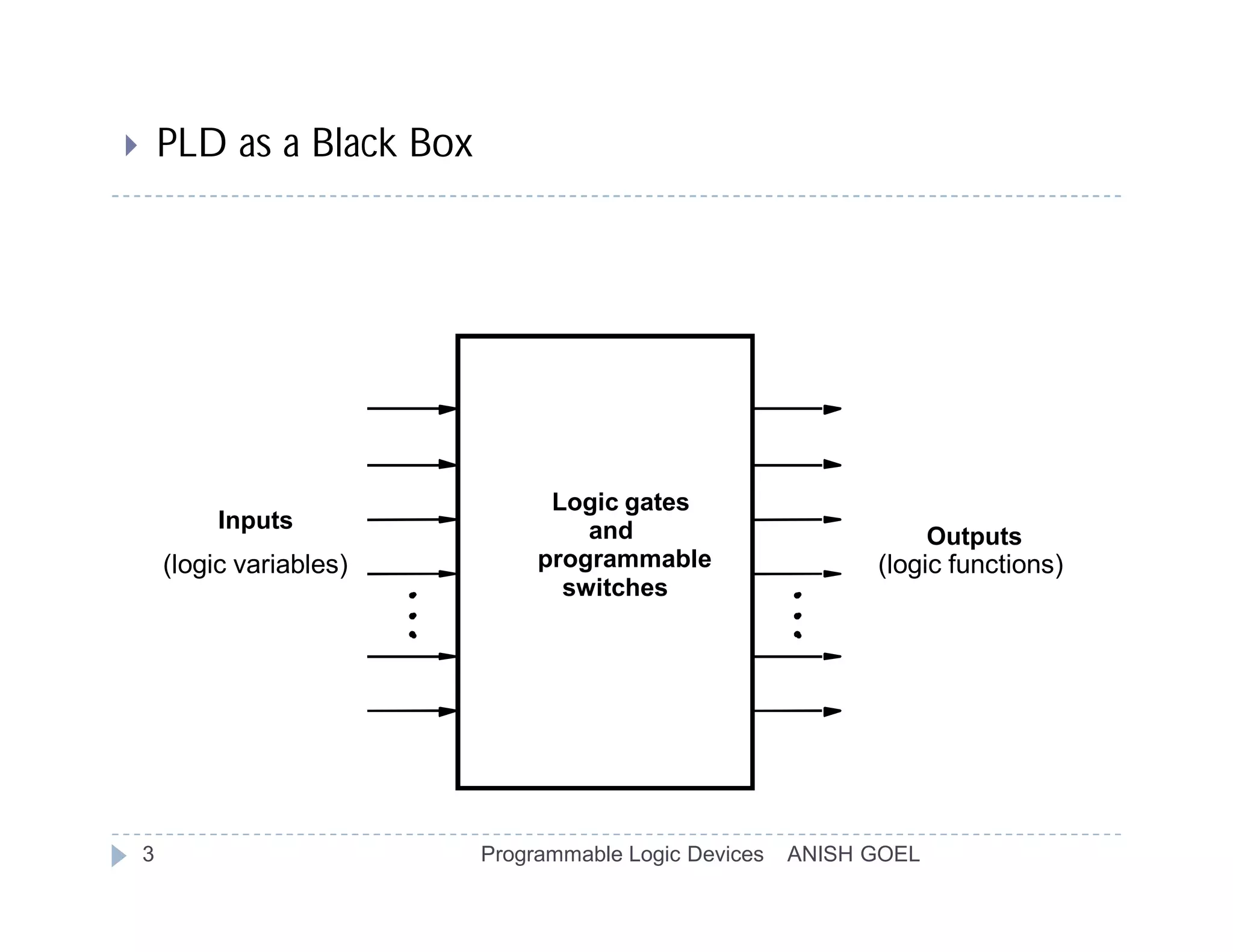
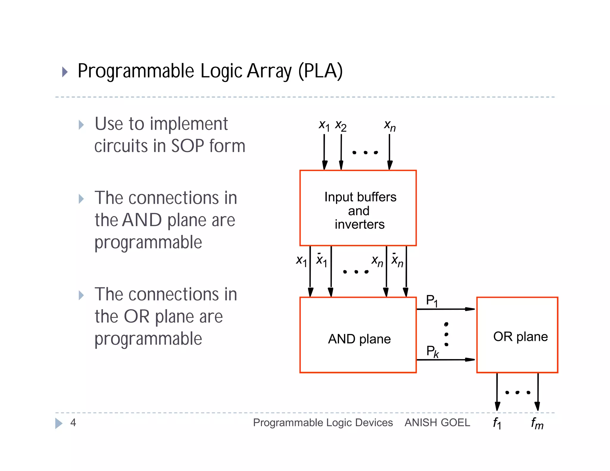
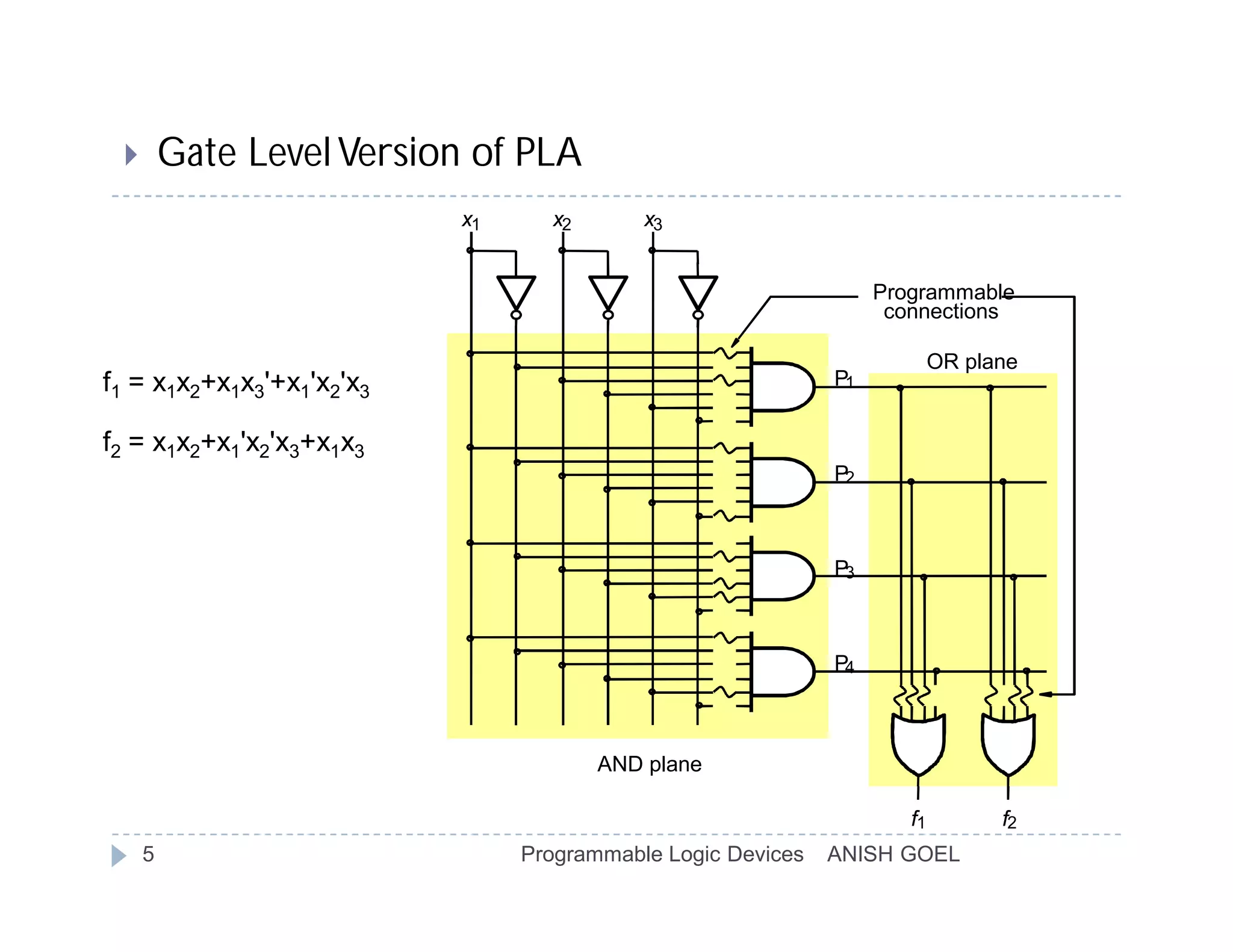
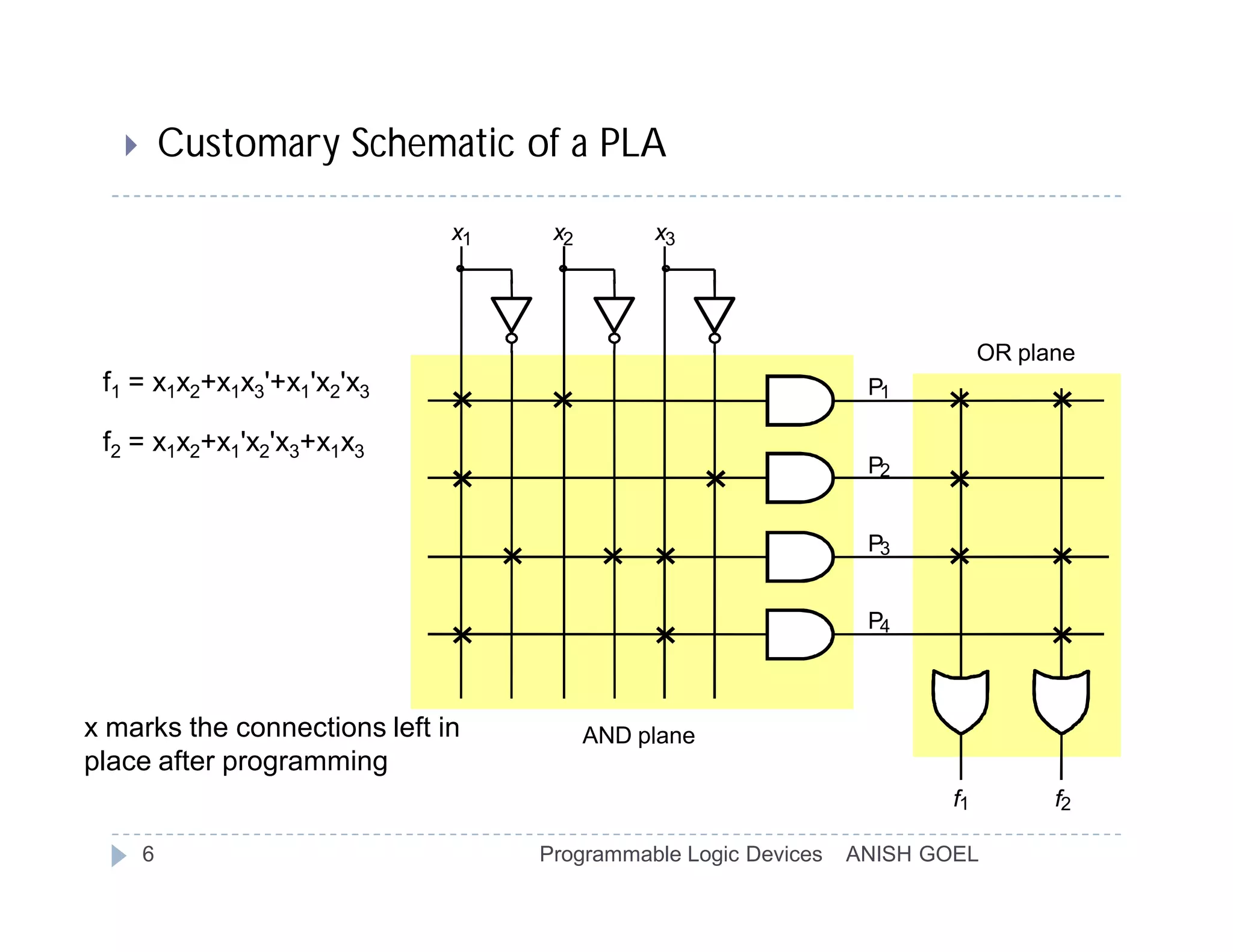
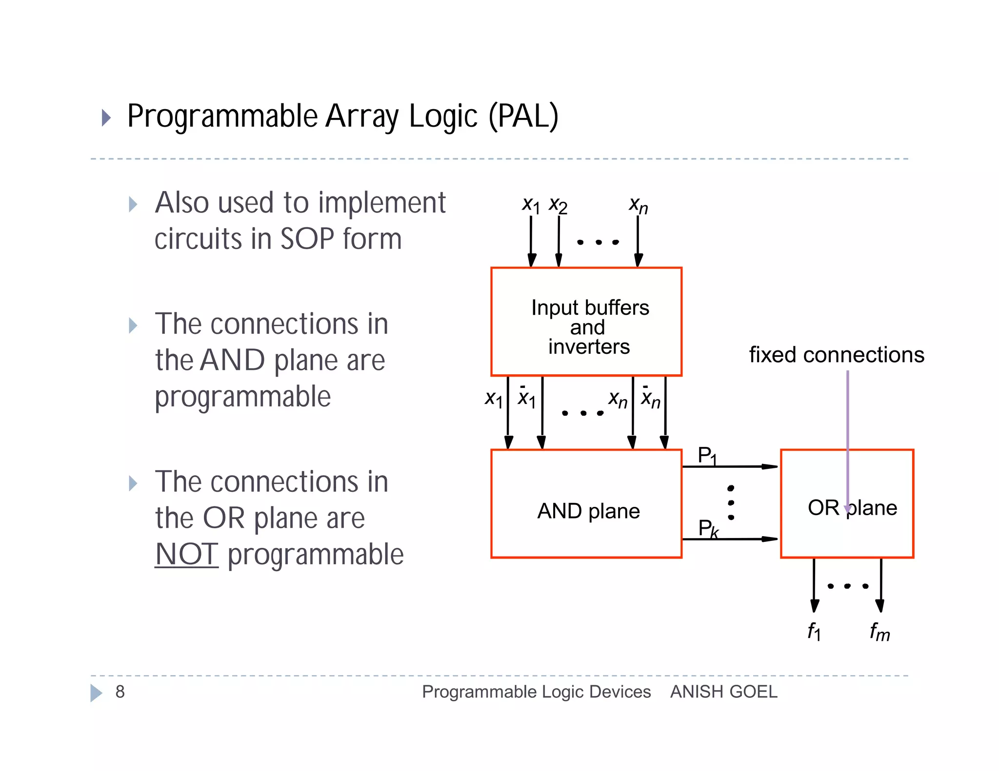
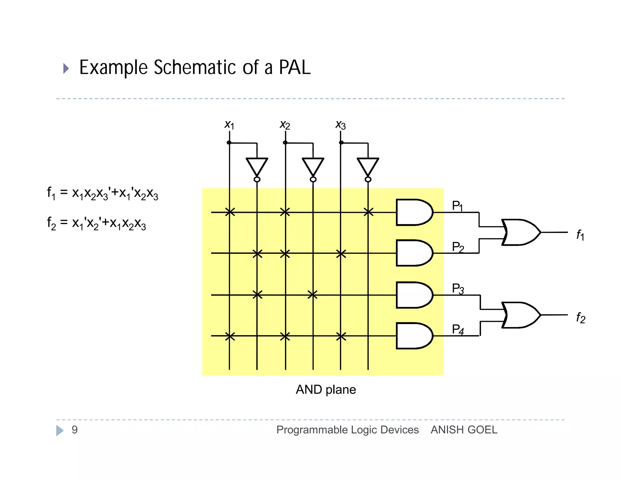
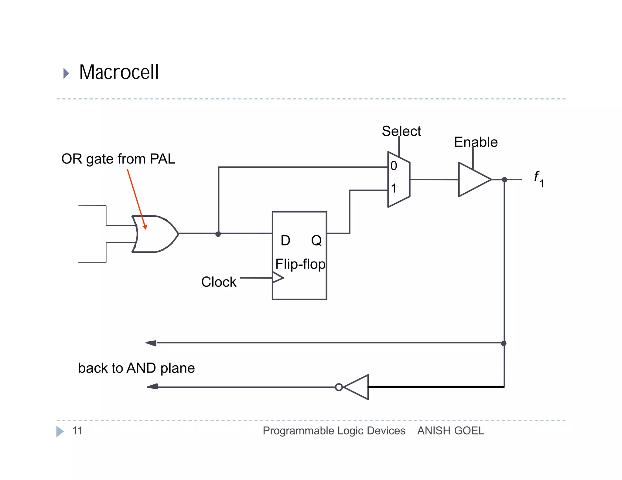
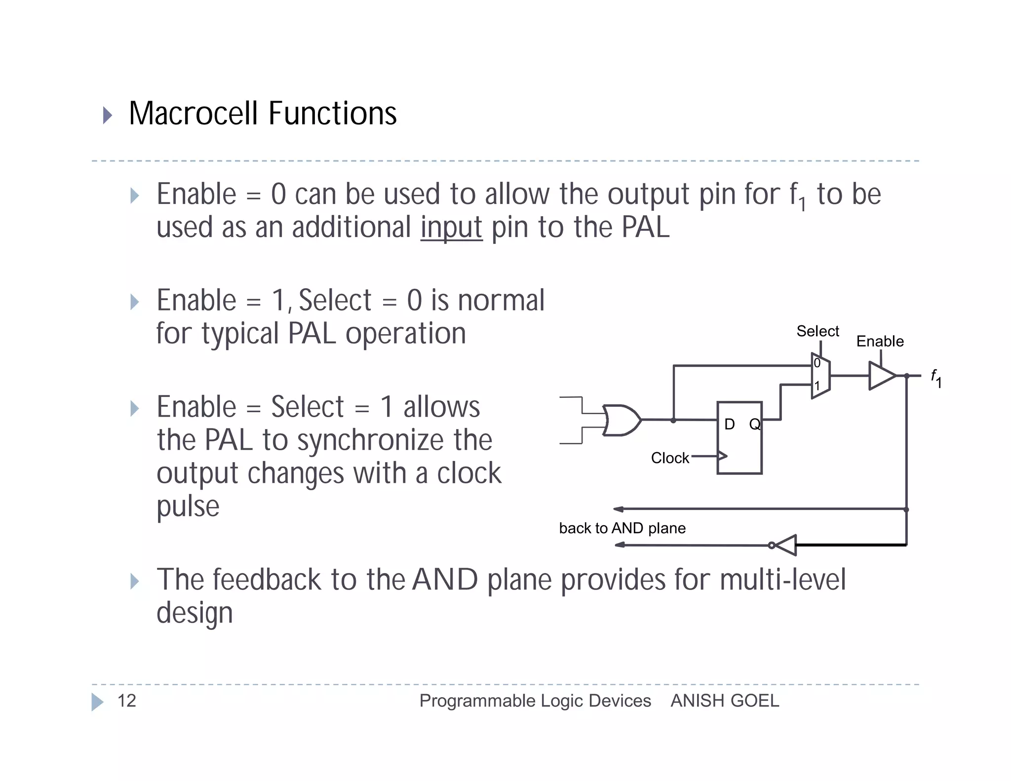
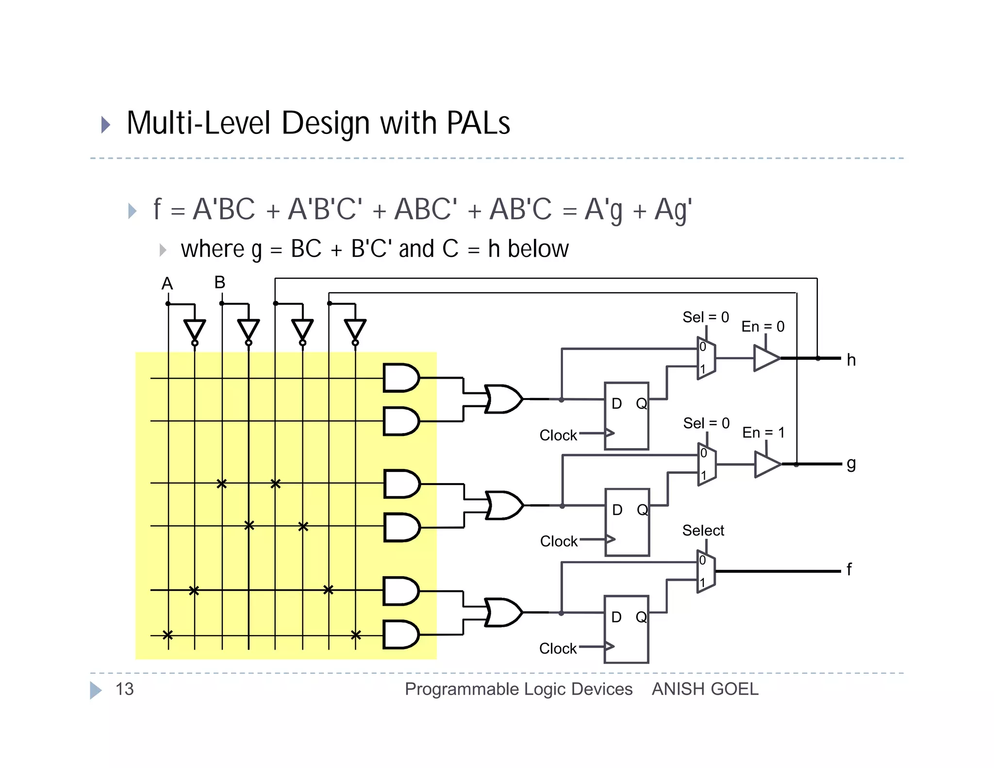
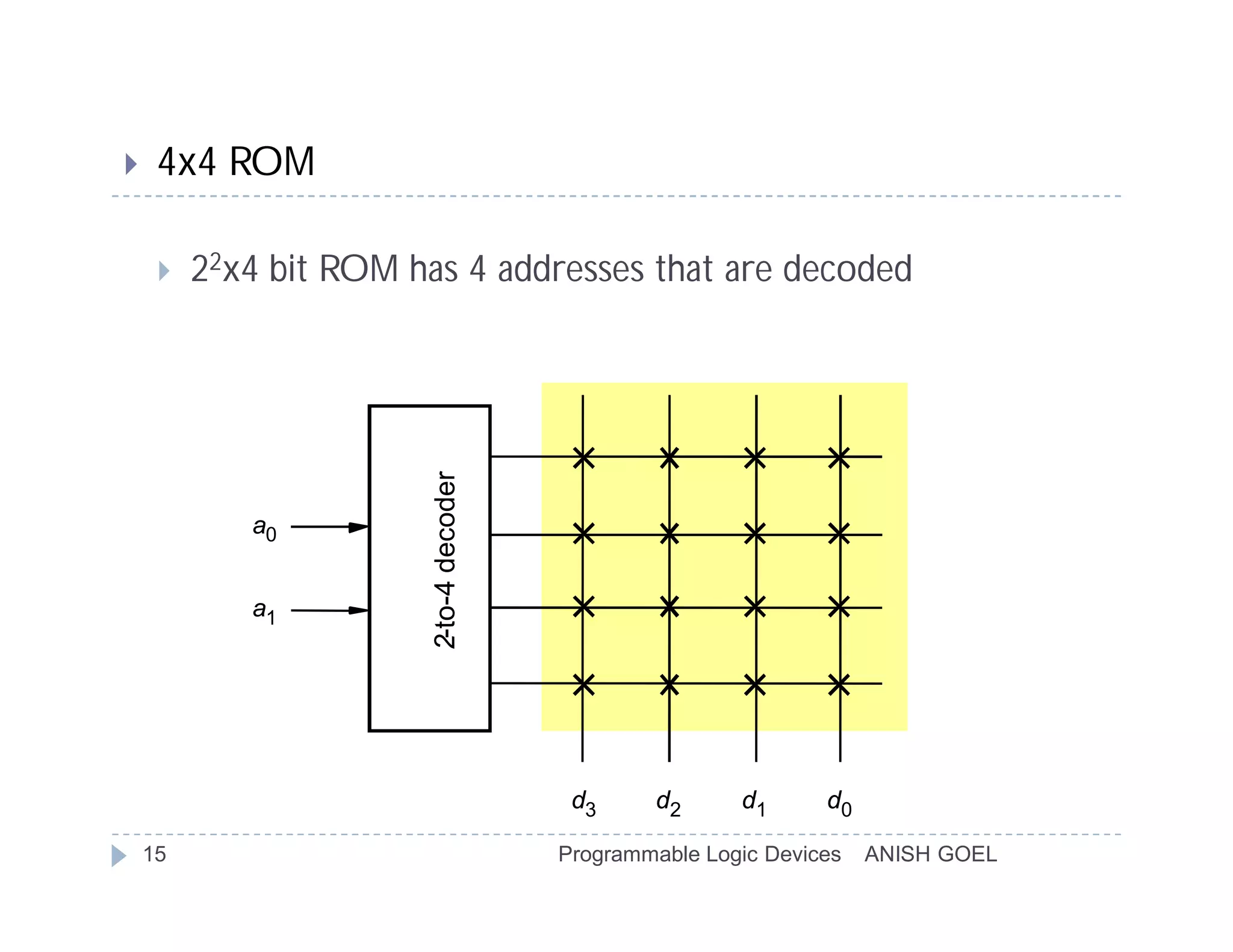
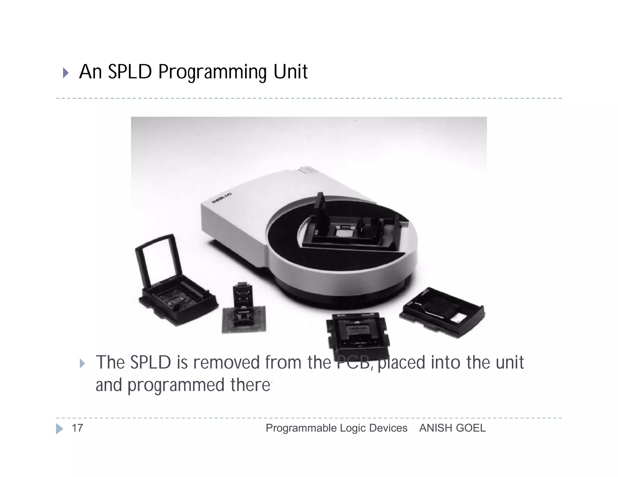
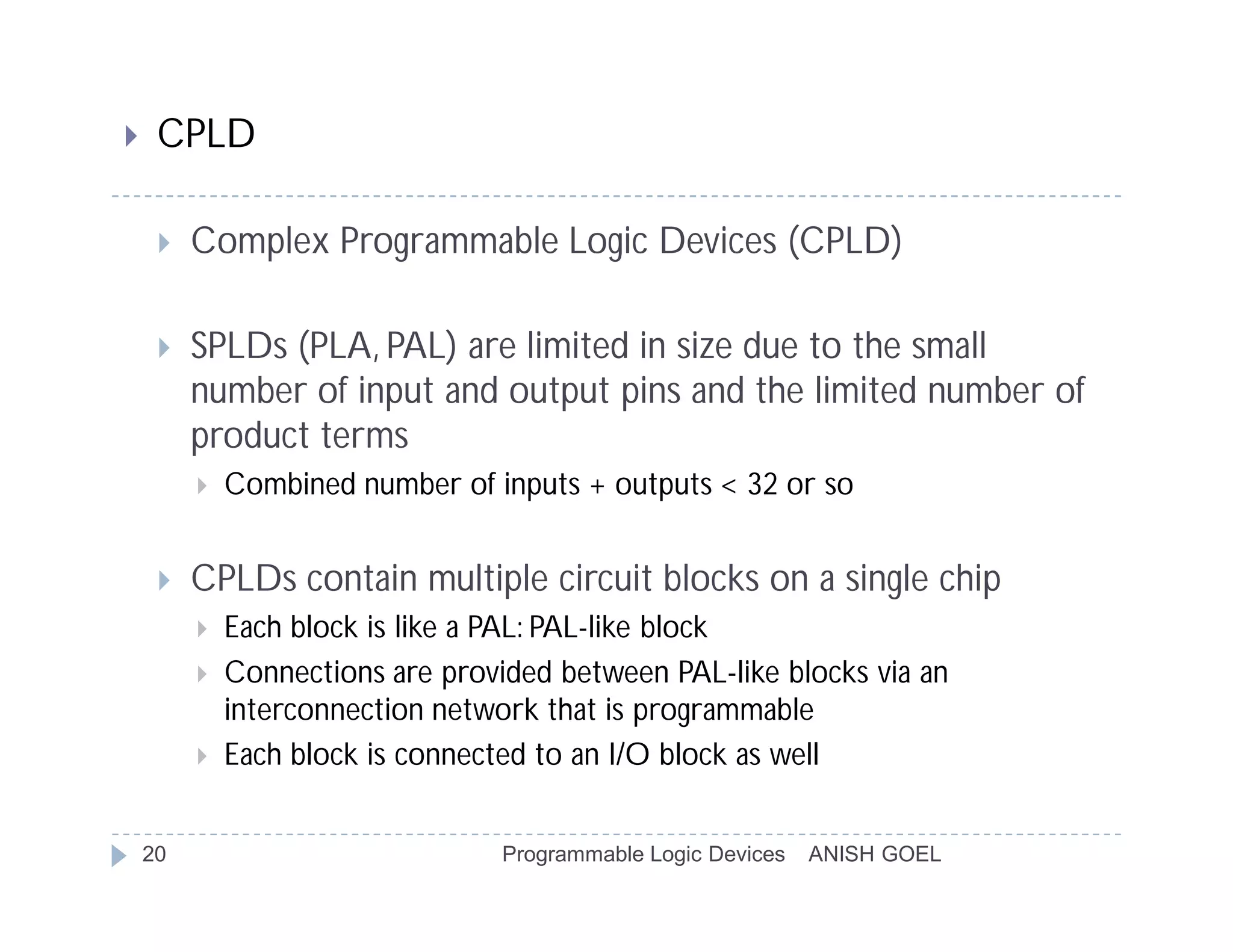
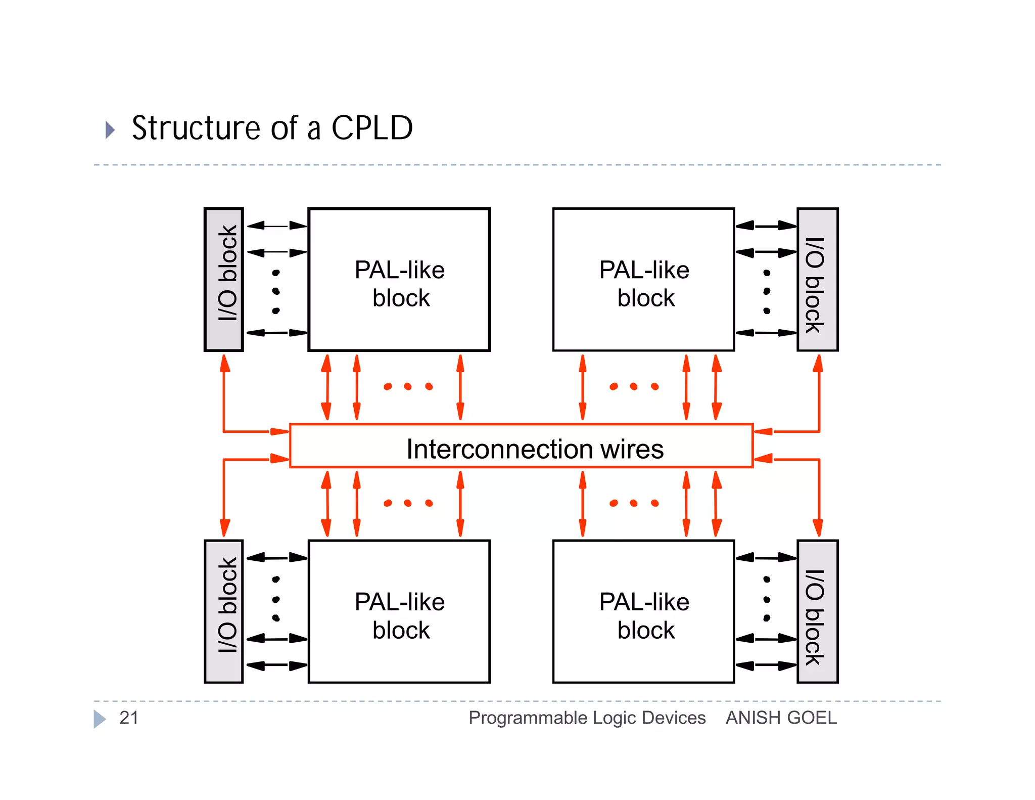
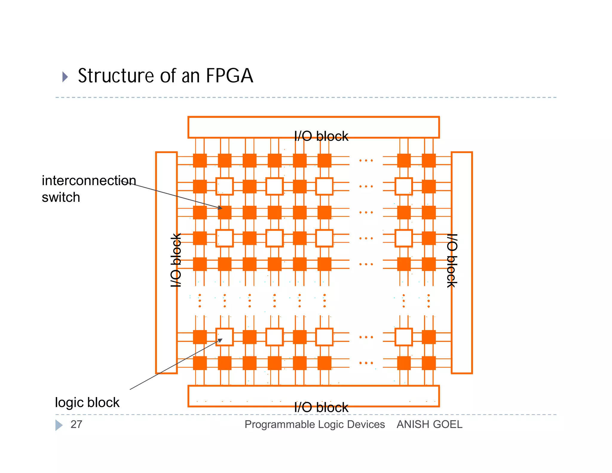
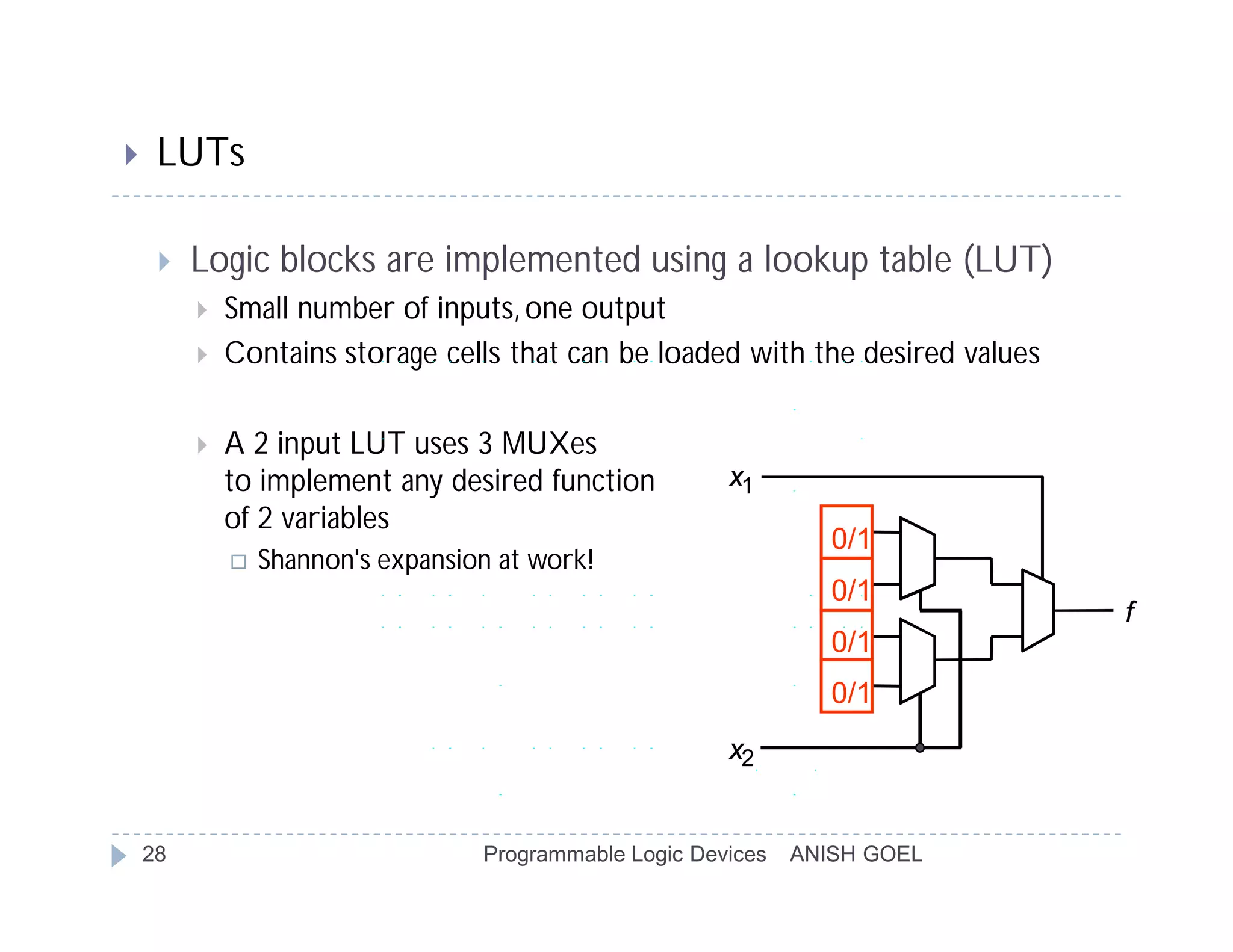
Programmable Logic Devices


           Prof. Anish Goel
Programmable Logic Devices

       Programmable Logic Devices (PLD)
           General purpose chip for implementing circuits
           Can be customized using programmable switches

       Main types of PLDs
           PLA
           PAL
           ROM
           CPLD
           FPGA

       Custom chips: standard cells, sea of gates

2                               Programmable Logic Devices   ANISH GOEL
       PLD as a Black Box


                                   Logic gates
             Inputs                   and                              Outputs
        (logic variables)         programmable                  (logic functions)
                                    switches


    3                        Programmable Logic Devices   ANISH GOEL
       Programmable Logic Array (PLA)

           Use to implement                   x1 x2       xn
            circuits in SOP form

           The connections in                  Input buffers
                                                    and
            the AND plane are                     inverters
            programmable
                                          x1 x1         xn xn

           The connections in                                     P1
            the OR plane are
            programmable                        AND plane                    OR plane
                                                                   Pk


    4                              Programmable Logic Devices   ANISH GOEL   f1   fm
       Gate Level Version of PLA
                           x1     x2       x3


                                                                  Programmable
                                                                   connections

                                                                          OR plane
f1 = x1x2+x1x3'+x1'x2'x3                                     P1


f2 = x1x2+x1'x2'x3+x1x3
                                                             P2


                                                             P3


                                                             P4


                                       AND plane

                                                                     f1         f2
     5                          Programmable Logic Devices   ANISH GOEL
       Customary Schematic of a PLA

                              x1    x2        x3


                                                                             OR plane
 f1 = x1x2+x1x3'+x1'x2'x3                                        P1

 f2 = x1x2+x1'x2'x3+x1x3
                                                                 P2


                                                                 P3


                                                                 P4


x marks the connections left in          AND plane
place after programming
                                                                        f1         f2

       6                           Programmable Logic Devices   ANISH GOEL
       Limitations of PLAs

           PLAs come in various sizes
               Typical size is 16 inputs, 32 product terms, 8 outputs
                   Each AND gate has large fan-in  this limits the number of inputs that can
                    be provided in a PLA

                   16 inputs  216 = possible input combinations; only 32 permitted (since 32
                    AND gates) in a typical PLA

                   32 AND terms permitted  large fan-in for OR gates as well
                     This makes PLAs slower and slightly more expensive than some
                       alternatives to be discussed shortly

                   8 outputs  could have shared minterms, but not required


    7                                      Programmable Logic Devices   ANISH GOEL
       Programmable Array Logic (PAL)

           Also used to implement          x1 x2       xn
            circuits in SOP form

                                             Input buffers
           The connections in                   and
                                               inverters             fixed connections
            the AND plane are
            programmable                x1 x1         xn xn

                                                                P1
           The connections in
                                              AND plane                    OR plane
            the OR plane are                                    Pk
            NOT programmable

                                                                           f1   fm

    8                            Programmable Logic Devices   ANISH GOEL
       Example Schematic of a PAL

                          x1    x2        x3


f1 = x1x2x3'+x1'x2x3
                                                                P1
f2 = x1'x2'+x1x2x3
                                                                          f1
                                                                P2


                                                                P3

                                                                          f2
                                                                P4


                                     AND plane


      9                         Programmable Logic Devices   ANISH GOEL
    Comparing PALs and PLAs

        PALs have the same limitations as PLAs (small number of
         allowed AND terms) plus they have a fixed OR plane  less
         flexibility than PLAs

        PALs are simpler to manufacture, cheaper, and faster (better
         performance)

        PALs also often have extra circuitry connected to the
         output of each OR gate
            The OR gate plus this circuitry is called a macrocell


    10                               Programmable Logic Devices   ANISH GOEL
    Macrocell

                                                      Select
                                                                   Enable
OR gate from PAL                                        0
                                                                            f1
                                                        1


                                    D    Q
                                   Flip-flop
                         Clock


     back to AND plane


    11                           Programmable Logic Devices   ANISH GOEL
    Macrocell Functions

        Enable = 0 can be used to allow the output pin for f1 to be
         used as an additional input pin to the PAL

        Enable = 1, Select = 0 is normal
         for typical PAL operation                                      Select
                                                                                 Enable
                                                                          0
                                                                                          f1
                                                                          1

        Enable = Select = 1 allows                              D Q
         the PAL to synchronize the                      Clock
         output changes with a clock
         pulse
                                             back to AND plane


        The feedback to the AND plane provides for multi-level
         design

    12                        Programmable Logic Devices   ANISH GOEL
    Multi-Level Design with PALs

        f = A'BC + A'B'C' + ABC' + AB'C = A'g + Ag'
            where g = BC + B'C' and C = h below
         A      B
                                                                Sel = 0
                                                                          En = 0
                                                                  0
                                                                  1
                                                                                   h

                                                        D Q
                                                                Sel = 0
                                                Clock                     En = 1
                                                                  0
                                                                                   g
                                                                  1

                                                        D Q
                                                                Select
                                                Clock
                                                                  0
                                                                                   f
                                                                  1

                                                        D Q

                                                Clock

    13                           Programmable Logic Devices   ANISH GOEL
    ROM

        A ROM (Read Only Memory) has a fixed AND plane and a
         programmable OR plane

        Size of AND plane is 2n where n = number of input pins
            Has an AND gate for every possible minterm so that all input
             combinations access a different AND gate


        OR plane dictates function mapped by the ROM


    14                              Programmable Logic Devices   ANISH GOEL
    4x4 ROM

        22x4 bit ROM has 4 addresses that are decoded


                        2-to-4 decoder

            a0


            a1


                                          d3     d2      d1      d0

    15                                   Programmable Logic Devices   ANISH GOEL
    Programming SPLDs

        PLAs, PALs, and ROMs are also called SPLDs – Simple
         Programmable Logic Devices

        SPLDs must be programmed so that the switches are in the
         correct places
            CAD tools are usually used to do this
                A fuse map is created by the CAD tool and then that map is downloaded
                 to the device via a special programming unit

            There are two basic types of programming techniques
                Removable sockets on a PCB
                In system programming (ISP) on a PCB
                   This approach is not very common for PLAs and PALs but it is quite
                    common for more complex PLDs


    16                              Programmable Logic Devices   ANISH GOEL
    An SPLD Programming Unit


        The SPLD is removed from the PCB, placed into the unit
         and programmed there

    17                        Programmable Logic Devices   ANISH GOEL
    Removable SPLD Socket Package

        PLCC (plastic-leaded chip carrier)


                                                                      PLCC socket soldered to
                                                                      the PCB


                                                                  d
                                                               oar
                                                        it b
                                                   i rcu
                                                 dc
                                              nte
                                       Pr i


    18                        Programmable Logic Devices                ANISH GOEL
    In System Programming (ISP)

        Used when the SPLD cannot be removed from the PCB

        A special cable and PCB connection are required to
         program the SPLD from an attached computer

        Very common approach to programming more complex
         PLDs like CPLDs, FPGAs, etc.


    19                      Programmable Logic Devices   ANISH GOEL
    CPLD

        Complex Programmable Logic Devices (CPLD)

        SPLDs (PLA, PAL) are limited in size due to the small
         number of input and output pins and the limited number of
         product terms
            Combined number of inputs + outputs < 32 or so


        CPLDs contain multiple circuit blocks on a single chip
            Each block is like a PAL: PAL-like block
            Connections are provided between PAL-like blocks via an
             interconnection network that is programmable
            Each block is connected to an I/O block as well


    20                            Programmable Logic Devices   ANISH GOEL
    Structure of a CPLD

          I/O block


                                                                    I/O block
                      PAL-like                 PAL-like
                       block                    block


                          Interconnection wires
          I/O block


                                                                    I/O block
                      PAL-like                 PAL-like
                       block                    block


    21                           Programmable Logic Devices   ANISH GOEL
    Internal Structure of a PAL-like Block

        Includes macrocells
            Usually about 16 each


        Fixed OR planes                            PAL-like block
            OR gates have fan-in
             between 5-20
                                                    PAL-like block

        XOR gates provide                                           DQ
         negation ability
                                                                     DQ
            XOR has a control
             input
                                                                     DQ


    22                               Programmable Logic Devices   ANISH GOEL
    More on PAL-like Blocks

        CPLD pins are provided to control XOR, MUX, and tri-state
         gates

        When tri-state gate is disabled, the corresponding output
         pin can be used as an input pin
            The associated PAL-like block is then useless


        The AND plane and interconnection network are
         programmable

        Commercial CPLDs have between 2-100 PAL-like blocks

    23                            Programmable Logic Devices   ANISH GOEL
    Programming a CPLD

        CPLDs have many pins – large ones have > 200
            Removal of CPLD from a PCB is difficult without breaking the pins
            Use ISP (in system programming) to program the CPLD
            JTAG (Joint Test Action Group) port used to connect the CPLD to a
             computer


    24                           Programmable Logic Devices   ANISH GOEL
    Example CPLD

        Use a CPLD to implement the function
            f = x1x3x6' + x1x4x5x6' + x2x3x7 + x2x4x5x7
               (from interconnection wires)
          x1      x2    x3    x4     x5       x6   x7   unused


                                                                     PAL-like block
                                                                                            0   1
                                                                          0
                                                                                                    f
                                                                                      D Q


    25                                                  Programmable Logic Devices    ANISH GOEL
    FPGA

        SPLDs and CPLDs are relatively small and useful for simple
         logic devices
            Up to about 20000 gates


        Field Programmable Gate Arrays (FPGA) can handle larger
         circuits
            No AND/OR planes
            Provide logic blocks, I/O blocks, and interconnection wires and
             switches

            Logic blocks provide functionality
            Interconnection switches allow logic blocks to be connected to each
             other and to the I/O pins

    26                            Programmable Logic Devices   ANISH GOEL
    Structure of an FPGA

                                       I/O block


interconnection
switch
                  I/O block


                                                                  I/O block
  logic block                          I/O block
       27                     Programmable Logic Devices   ANISH GOEL
    LUTs

        Logic blocks are implemented using a lookup table (LUT)
            Small number of inputs, one output
            Contains storage cells that can be loaded with the desired values

            A 2 input LUT uses 3 MUXes
             to implement any desired function           x1
             of 2 variables
                                                                   0/1
                Shannon's expansion at work!
                                                                   0/1
                                                                                 f
                                                                   0/1
                                                                   0/1
                                                         x2


    28                             Programmable Logic Devices   ANISH GOEL
    Example 2 Input LUT


         x1   x2   f
         0    0    1        f = x1'x2' + x1x2, or using Shannon's expansion:
         0    1    0
                            f = x1'(x2') + x1(x2)
         1    0    0
                              = x1'(x2'(1) + x2(0)) + x1(x2'(0) + x2(1))
         1    1    1
                       x1

                               1
                               0
                                                              f
                               0
                               1

                       x2

    29                          Programmable Logic Devices   ANISH GOEL
    3 Input LUT
                                 x1
        7 2x1 MUXes and         x2
         8 storage cells are
         required                          0/1
                                           0/1

        Commercial LUTs have              0/1
         4-5 inputs, and 16-32             0/1
                                                                         f
         storage cells                     0/1
                                           0/1
                                           0/1
                                           0/1
                                 x3

    30                         Programmable Logic Devices   ANISH GOEL
    Programming an FPGA

        ISP method is used

        LUTs contain volatile storage cells
            None of the other PLD technologies are volatile
            FPGA storage cells are loaded via a PROM when power is first applied


        The UP2 Education Board by Altera contains a JTAG port, a
         MAX 7000 CPLD, and a FLEX 10K FPGA
            The MAX 7000 CPLD chip is EPM7128SLC84-7
            EPM7  MAX 7000 family; 128 macrocells; LC84  84 pin PLCC
             package; 7  speed grade


    31                             Programmable Logic Devices   ANISH GOEL
    Example FPGA

        Use an FPGA with 2 input LUTS to implement the function f
         = x1x2 + x2'x3             x      3           f


          f1   = x 1x 2
                            x1
            f2 = x2'x3
                                           x1 0                 x2 0
            f = f1 + f 2                     0   f1               1   f2
                                              0                    0
                            x2             x2                   x3
                                              1                    0


                                                                f1 0
                                                                   1   f
                                                                   1
                                                                f2
                                                                   1


    32                           Programmable Logic Devices   ANISH GOEL
    Another Example FPGA

        Use an FPGA with 2 input LUTS to implement the function f
         = x1x3x6' + x1x4x5x6' + x2x3x7 + x2x4x5x7

            Fan-in of expression is too large for FPGA (this was simple to do in a
             CPLD)

            Factor f to get sub-expressions with max fan-in = 2
                f = x1x6'(x3 + x4x5) + x2x7(x3 + x4x5)
                   = (x1x6' + x2x7)(x3 + x4x5)


            Could use Shannon's expansion instead
                Goal is to build expressions out of 2-input LUTs


    33                               Programmable Logic Devices   ANISH GOEL
    FPGA Implementation

        f = (x1x6' + x2x7)(xx3 + x4x5)        x5                   x3
                               4                                          f


            x1

                        x1 0                    x4 0                x3 0
                           0   A                   0 C                 1 E
            x6          x6 1                    x5 0                C 1
                                                                       1
                           0                       1


            x2

                        x2 0                    A   0               D 0
                           0   B                    1 D               0   f
            x7          x7 0                    B
                                                    1                 0
                                                                    E 1
                           1                        1


    34                             Programmable Logic Devices   ANISH GOEL
    Custom Chips

        PLDs are limited by number of programmable switches
            Consume space
            Reduce speed


        Custom chips are created from scratch
            Expensive  used when high speed is required, volume sales are
             expected, and chip size is small but with high density of gates
            ASICs (Application Specific Integrated Circuits) are custom chips that
             use a standard cell layout to reduce design costs


    35                              Programmable Logic Devices   ANISH GOEL
    Standard Cells

        Rows of logic gates can be connected by wires in the routing
         channels
            Designers (via CAD tools) select prefab gates from a library and place
             them in rows
            Interconnections are made by wires in routing channels
                Multiple layers may be used to avoid short circuiting
                A hard-wired connection between layers is called a via


                     x1                                                      f2

                     x2

                     x3
                                                                             f1


    36                                  Programmable Logic Devices   ANISH GOEL
    Example: Standard Cells

      f1   = x1x2 + x1'x2'x3 + x1x3'
        f2 = x1x2 + x1'x2'x3 + x1x3


         x1                                                                 f2

         x2
         x3
                                                                            f1


    37                            Programmable Logic Devices   ANISH GOEL
    Sea of Gates Gate Array

        A Sea of Gates gate array is just like a standard cell except
         all gates are of the same type
            Interconnections are run in channels and use multiple layers
            Cheaper to manufacture due to regularity


    38                            Programmable Logic Devices   ANISH GOEL
    Example: Sea of Gates

        f1   = x2x3' + x1x3                                             black  bottom
                                                                         layer channels


red  top layer channels

      39                       Programmable Logic Devices   ANISH GOEL
    Digital Logic Technology Tradeoffs


                                                               Full custom
                                                               VLSI design


                                                       ASICs
Speed / Density /
Complexity / Likely
Market Volume                          CPLDs
                                       FPGAs


                           PLDs


                         Engineering cost / Time to develop
      40                  Programmable Logic Devices   ANISH GOEL

PLD's

  • 1.
  • 2.
    Programmable Logic Devices  Programmable Logic Devices (PLD)  General purpose chip for implementing circuits  Can be customized using programmable switches  Main types of PLDs  PLA  PAL  ROM  CPLD  FPGA  Custom chips: standard cells, sea of gates 2 Programmable Logic Devices ANISH GOEL
  • 3.
    PLD as a Black Box Logic gates Inputs and Outputs (logic variables) programmable (logic functions) switches 3 Programmable Logic Devices ANISH GOEL
  • 4.
    Programmable Logic Array (PLA)  Use to implement x1 x2 xn circuits in SOP form  The connections in Input buffers and the AND plane are inverters programmable x1 x1 xn xn  The connections in P1 the OR plane are programmable AND plane OR plane Pk 4 Programmable Logic Devices ANISH GOEL f1 fm
  • 5.
    Gate Level Version of PLA x1 x2 x3 Programmable connections OR plane f1 = x1x2+x1x3'+x1'x2'x3 P1 f2 = x1x2+x1'x2'x3+x1x3 P2 P3 P4 AND plane f1 f2 5 Programmable Logic Devices ANISH GOEL
  • 6.
    Customary Schematic of a PLA x1 x2 x3 OR plane f1 = x1x2+x1x3'+x1'x2'x3 P1 f2 = x1x2+x1'x2'x3+x1x3 P2 P3 P4 x marks the connections left in AND plane place after programming f1 f2 6 Programmable Logic Devices ANISH GOEL
  • 7.
    Limitations of PLAs  PLAs come in various sizes  Typical size is 16 inputs, 32 product terms, 8 outputs  Each AND gate has large fan-in  this limits the number of inputs that can be provided in a PLA  16 inputs  216 = possible input combinations; only 32 permitted (since 32 AND gates) in a typical PLA  32 AND terms permitted  large fan-in for OR gates as well  This makes PLAs slower and slightly more expensive than some alternatives to be discussed shortly  8 outputs  could have shared minterms, but not required 7 Programmable Logic Devices ANISH GOEL
  • 8.
    Programmable Array Logic (PAL)  Also used to implement x1 x2 xn circuits in SOP form Input buffers  The connections in and inverters fixed connections the AND plane are programmable x1 x1 xn xn P1  The connections in AND plane OR plane the OR plane are Pk NOT programmable f1 fm 8 Programmable Logic Devices ANISH GOEL
  • 9.
    Example Schematic of a PAL x1 x2 x3 f1 = x1x2x3'+x1'x2x3 P1 f2 = x1'x2'+x1x2x3 f1 P2 P3 f2 P4 AND plane 9 Programmable Logic Devices ANISH GOEL
  • 10.
    Comparing PALs and PLAs  PALs have the same limitations as PLAs (small number of allowed AND terms) plus they have a fixed OR plane  less flexibility than PLAs  PALs are simpler to manufacture, cheaper, and faster (better performance)  PALs also often have extra circuitry connected to the output of each OR gate  The OR gate plus this circuitry is called a macrocell 10 Programmable Logic Devices ANISH GOEL
  • 11.
    Macrocell Select Enable OR gate from PAL 0 f1 1 D Q Flip-flop Clock back to AND plane 11 Programmable Logic Devices ANISH GOEL
  • 12.
    Macrocell Functions  Enable = 0 can be used to allow the output pin for f1 to be used as an additional input pin to the PAL  Enable = 1, Select = 0 is normal for typical PAL operation Select Enable 0 f1 1  Enable = Select = 1 allows D Q the PAL to synchronize the Clock output changes with a clock pulse back to AND plane  The feedback to the AND plane provides for multi-level design 12 Programmable Logic Devices ANISH GOEL
  • 13.
    Multi-Level Design with PALs  f = A'BC + A'B'C' + ABC' + AB'C = A'g + Ag'  where g = BC + B'C' and C = h below A B Sel = 0 En = 0 0 1 h D Q Sel = 0 Clock En = 1 0 g 1 D Q Select Clock 0 f 1 D Q Clock 13 Programmable Logic Devices ANISH GOEL
  • 14.
    ROM  A ROM (Read Only Memory) has a fixed AND plane and a programmable OR plane  Size of AND plane is 2n where n = number of input pins  Has an AND gate for every possible minterm so that all input combinations access a different AND gate  OR plane dictates function mapped by the ROM 14 Programmable Logic Devices ANISH GOEL
  • 15.
    4x4 ROM  22x4 bit ROM has 4 addresses that are decoded 2-to-4 decoder a0 a1 d3 d2 d1 d0 15 Programmable Logic Devices ANISH GOEL
  • 16.
    Programming SPLDs  PLAs, PALs, and ROMs are also called SPLDs – Simple Programmable Logic Devices  SPLDs must be programmed so that the switches are in the correct places  CAD tools are usually used to do this  A fuse map is created by the CAD tool and then that map is downloaded to the device via a special programming unit  There are two basic types of programming techniques  Removable sockets on a PCB  In system programming (ISP) on a PCB  This approach is not very common for PLAs and PALs but it is quite common for more complex PLDs 16 Programmable Logic Devices ANISH GOEL
  • 17.
    An SPLD Programming Unit  The SPLD is removed from the PCB, placed into the unit and programmed there 17 Programmable Logic Devices ANISH GOEL
  • 18.
    Removable SPLD Socket Package  PLCC (plastic-leaded chip carrier) PLCC socket soldered to the PCB d oar it b i rcu dc nte Pr i 18 Programmable Logic Devices ANISH GOEL
  • 19.
    In System Programming (ISP)  Used when the SPLD cannot be removed from the PCB  A special cable and PCB connection are required to program the SPLD from an attached computer  Very common approach to programming more complex PLDs like CPLDs, FPGAs, etc. 19 Programmable Logic Devices ANISH GOEL
  • 20.
    CPLD  Complex Programmable Logic Devices (CPLD)  SPLDs (PLA, PAL) are limited in size due to the small number of input and output pins and the limited number of product terms  Combined number of inputs + outputs < 32 or so  CPLDs contain multiple circuit blocks on a single chip  Each block is like a PAL: PAL-like block  Connections are provided between PAL-like blocks via an interconnection network that is programmable  Each block is connected to an I/O block as well 20 Programmable Logic Devices ANISH GOEL
  • 21.
    Structure of a CPLD I/O block I/O block PAL-like PAL-like block block Interconnection wires I/O block I/O block PAL-like PAL-like block block 21 Programmable Logic Devices ANISH GOEL
  • 22.
    Internal Structure of a PAL-like Block  Includes macrocells  Usually about 16 each  Fixed OR planes PAL-like block  OR gates have fan-in between 5-20 PAL-like block  XOR gates provide DQ negation ability DQ  XOR has a control input DQ 22 Programmable Logic Devices ANISH GOEL
  • 23.
    More on PAL-like Blocks  CPLD pins are provided to control XOR, MUX, and tri-state gates  When tri-state gate is disabled, the corresponding output pin can be used as an input pin  The associated PAL-like block is then useless  The AND plane and interconnection network are programmable  Commercial CPLDs have between 2-100 PAL-like blocks 23 Programmable Logic Devices ANISH GOEL
  • 24.
    Programming a CPLD  CPLDs have many pins – large ones have > 200  Removal of CPLD from a PCB is difficult without breaking the pins  Use ISP (in system programming) to program the CPLD  JTAG (Joint Test Action Group) port used to connect the CPLD to a computer 24 Programmable Logic Devices ANISH GOEL
  • 25.
    Example CPLD  Use a CPLD to implement the function  f = x1x3x6' + x1x4x5x6' + x2x3x7 + x2x4x5x7 (from interconnection wires) x1 x2 x3 x4 x5 x6 x7 unused PAL-like block 0 1 0 f D Q 25 Programmable Logic Devices ANISH GOEL
  • 26.
    FPGA  SPLDs and CPLDs are relatively small and useful for simple logic devices  Up to about 20000 gates  Field Programmable Gate Arrays (FPGA) can handle larger circuits  No AND/OR planes  Provide logic blocks, I/O blocks, and interconnection wires and switches  Logic blocks provide functionality  Interconnection switches allow logic blocks to be connected to each other and to the I/O pins 26 Programmable Logic Devices ANISH GOEL
  • 27.
    Structure of an FPGA I/O block interconnection switch I/O block I/O block logic block I/O block 27 Programmable Logic Devices ANISH GOEL
  • 28.
    LUTs  Logic blocks are implemented using a lookup table (LUT)  Small number of inputs, one output  Contains storage cells that can be loaded with the desired values  A 2 input LUT uses 3 MUXes to implement any desired function x1 of 2 variables 0/1  Shannon's expansion at work! 0/1 f 0/1 0/1 x2 28 Programmable Logic Devices ANISH GOEL
  • 29.
    Example 2 Input LUT x1 x2 f 0 0 1 f = x1'x2' + x1x2, or using Shannon's expansion: 0 1 0 f = x1'(x2') + x1(x2) 1 0 0 = x1'(x2'(1) + x2(0)) + x1(x2'(0) + x2(1)) 1 1 1 x1 1 0 f 0 1 x2 29 Programmable Logic Devices ANISH GOEL
  • 30.
    3 Input LUT x1  7 2x1 MUXes and x2 8 storage cells are required 0/1 0/1  Commercial LUTs have 0/1 4-5 inputs, and 16-32 0/1 f storage cells 0/1 0/1 0/1 0/1 x3 30 Programmable Logic Devices ANISH GOEL
  • 31.
    Programming an FPGA  ISP method is used  LUTs contain volatile storage cells  None of the other PLD technologies are volatile  FPGA storage cells are loaded via a PROM when power is first applied  The UP2 Education Board by Altera contains a JTAG port, a MAX 7000 CPLD, and a FLEX 10K FPGA  The MAX 7000 CPLD chip is EPM7128SLC84-7  EPM7  MAX 7000 family; 128 macrocells; LC84  84 pin PLCC package; 7  speed grade 31 Programmable Logic Devices ANISH GOEL
  • 32.
    Example FPGA  Use an FPGA with 2 input LUTS to implement the function f = x1x2 + x2'x3 x 3 f  f1 = x 1x 2 x1  f2 = x2'x3 x1 0 x2 0  f = f1 + f 2 0 f1 1 f2 0 0 x2 x2 x3 1 0 f1 0 1 f 1 f2 1 32 Programmable Logic Devices ANISH GOEL
  • 33.
    Another Example FPGA  Use an FPGA with 2 input LUTS to implement the function f = x1x3x6' + x1x4x5x6' + x2x3x7 + x2x4x5x7  Fan-in of expression is too large for FPGA (this was simple to do in a CPLD)  Factor f to get sub-expressions with max fan-in = 2  f = x1x6'(x3 + x4x5) + x2x7(x3 + x4x5) = (x1x6' + x2x7)(x3 + x4x5)  Could use Shannon's expansion instead  Goal is to build expressions out of 2-input LUTs 33 Programmable Logic Devices ANISH GOEL
  • 34.
    FPGA Implementation  f = (x1x6' + x2x7)(xx3 + x4x5) x5 x3 4 f x1 x1 0 x4 0 x3 0 0 A 0 C 1 E x6 x6 1 x5 0 C 1 1 0 1 x2 x2 0 A 0 D 0 0 B 1 D 0 f x7 x7 0 B 1 0 E 1 1 1 34 Programmable Logic Devices ANISH GOEL
  • 35.
    Custom Chips  PLDs are limited by number of programmable switches  Consume space  Reduce speed  Custom chips are created from scratch  Expensive  used when high speed is required, volume sales are expected, and chip size is small but with high density of gates  ASICs (Application Specific Integrated Circuits) are custom chips that use a standard cell layout to reduce design costs 35 Programmable Logic Devices ANISH GOEL
  • 36.
    Standard Cells  Rows of logic gates can be connected by wires in the routing channels  Designers (via CAD tools) select prefab gates from a library and place them in rows  Interconnections are made by wires in routing channels  Multiple layers may be used to avoid short circuiting  A hard-wired connection between layers is called a via x1 f2 x2 x3 f1 36 Programmable Logic Devices ANISH GOEL
  • 37.
    Example: Standard Cells  f1 = x1x2 + x1'x2'x3 + x1x3'  f2 = x1x2 + x1'x2'x3 + x1x3 x1 f2 x2 x3 f1 37 Programmable Logic Devices ANISH GOEL
  • 38.
    Sea of Gates Gate Array  A Sea of Gates gate array is just like a standard cell except all gates are of the same type  Interconnections are run in channels and use multiple layers  Cheaper to manufacture due to regularity 38 Programmable Logic Devices ANISH GOEL
  • 39.
    Example: Sea of Gates  f1 = x2x3' + x1x3 black  bottom layer channels red  top layer channels 39 Programmable Logic Devices ANISH GOEL
  • 40.
    Digital Logic Technology Tradeoffs Full custom VLSI design ASICs Speed / Density / Complexity / Likely Market Volume CPLDs FPGAs PLDs Engineering cost / Time to develop 40 Programmable Logic Devices ANISH GOEL