Downloaded 2,760 times

![Dr.Y.NARASIMHA MURTHY Ph.D
yayavaram@yahoo.com
PROGRAM
#include <LPC2148.H> // 2148 Header
#include "SPIsw.h"
unsigned long DACval, DACreg;
int main (void) // Main program
{
PINSEL0 = 0 ; // Port 0 as GPIO
PINSEL1 = 0x0000 ; // Port 0 as Outport
PINSEL2 & = 0x0000000C;
SPI_ init (&IOPIN0,29/*CS*/, 5/*MISO*/, 6/*MOSI*/, 4/*SCK*/, 0/*CPOL*/, 0/*CPHA*/) ;
// Set output voltage
DAC val = 2047 ; // Range [0..4095]
DAC reg = DACval | 0x7000 ;
SPI_enable () ; // Enable SPI port
SPI_char ((DACreg >> 8) & 0x00FF);
SPI_char (DACreg & 0x00FF) ;
SPI_disable () ; // Disable SPI port
while (1) ; // Infinite Loop
}
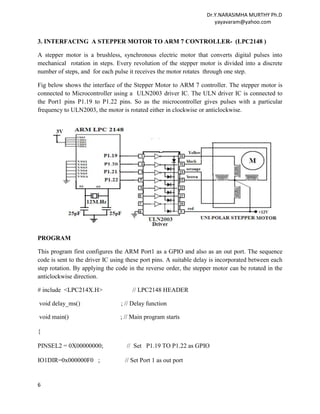
5. INTERFACING ADC –LPC2148
LPC2148 controller has two on n-chip ADCs. In the present program the ADC0 with channel 3
is used and configured to convert the analog input signal into its equivalent digital output.The
configuring of on chip ADC is shown below.
9](https://image.slidesharecdn.com/arm7-examplesfinal-130415124707-phpapp02/85/Arm7-Interfacing-examples-9-320.jpg)

![Dr.Y.NARASIMHA MURTHY Ph.D
yayavaram@yahoo.com
PROGRAM
#include<lpc21xx.h>
unsigned char seg[16] ={0x40,0x79,0x24,0x30,0x19,0x12,0x02,0x78,0x00,0x10,0x08,
0x03,0x46,0x21,0x06,0x0e};
unsigned char seg_val,seg_val1;
unsigned char count,count1;
unsigned long int var,var1;
void main(void)
{ unsigned long int k;
PINSEL0=0X00000000; // Select Port 0 pins as GPIO lines
12](https://image.slidesharecdn.com/arm7-examplesfinal-130415124707-phpapp02/85/Arm7-Interfacing-examples-12-320.jpg)
![Dr.Y.NARASIMHA MURTHY Ph.D
yayavaram@yahoo.com
PINSEL1=0X00000000; // Select Port 1 pins as GPIO lines
IODIR0 = 0X00FF0000; // Configure the required pins of Port 0 as output pins
IODIR1 = 0X00FF0000; // Configure the required pins of Port 1 as output pins
for (count=0;count<=15;count++) // COUNT FOR MSB
{ IOCLR1 = var;
seg_val = seg[count];
var = seg_val;
var = var<<16;
IOSET1 = var;
for(count1=0;count1<=15;count1++) // COUNT FOR LSB
{ IOCLR0=var1;
seg_val1=seg[count1];
var1=seg_val1;
var1=var1<<16;
IOSET0=var1;
for(k=0;k<50000;k++);
} // End for loop
} // End for loop
} // End main.
13](https://image.slidesharecdn.com/arm7-examplesfinal-130415124707-phpapp02/85/Arm7-Interfacing-examples-13-320.jpg)
![Dr.Y.NARASIMHA MURTHY Ph.D
yayavaram@yahoo.com
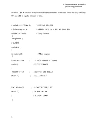
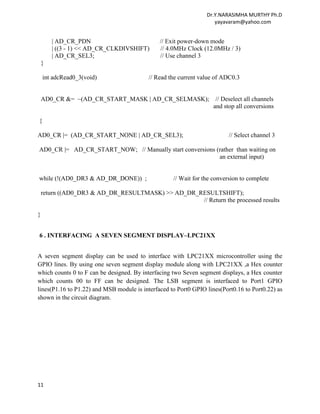
7 . INTERFACING OF 2X16 LCD MODULE - LPC21XX
The ARM7 LPC21xx processor is interfaced to the 2x16 LCD mpdule in 4-bit mode .The
interfcae diagram is shown below.The four data pins are connected with 4 data bits (P0.19 –
P0.22 pins to bits D4-D7), address bit (RS-P0.16), read/write bit (R/W-P0.17) and control
signal (E-P0.18) to make LCD display complete.The pins D0,D1,D2,D3 are left free with out
any connections.
16X 2 LCD is a 16 pin module . In which pins 1 &16 are grounded, 2 &15 are given to V CC
and 3rd pin is given to potentiometer in order adjust the contrast of LCD. Pins 4, 5 & 6
corresponds to RS, R/W & EN respectively. Pins 7 to 14 are data lines from D0 to D7
respectively. Here the LCD is used in 4 bit mode i.e. upper 4 bits are used to transfer the data
with MSB first and LSB next. Port 0 pins i.e. from P0.16 to P0.22 are used for both data and
control signals. The interfacing diagram of 16X2 LCD is shown below.
PROGRAM
#include <LPC21xx.H>
long unsigned int data,temp1,temp2;
unsigned char *ptr,data_array[] = "SSBN DEGREE & PG COLLEGE, ATP";
void main()
{
int i=0;
14](https://image.slidesharecdn.com/arm7-examplesfinal-130415124707-phpapp02/85/Arm7-Interfacing-examples-14-320.jpg)
![Dr.Y.NARASIMHA MURTHY Ph.D
yayavaram@yahoo.com
PINSEL0 = 0x00000000; // Select Port 0 pins as GPIO lines
IODIR0 = 0x00ff0000; // Configure the required pins of Port 0 as output pins
lcd_init(); // LCD initialization
delay(2500); // Delay
ret_home(); // Cursor to return home
delay(2500); // Delay
clr_disp(); // Clear display
delay(2500); // Delay
ptr = &data_array[0];
for(i=1;i<sizeof(data_array);i++)
{
if(i == 17)
{ temp1 = 0xc0; // Goto 2nd line in the LCD
lcd_com(); // Byte to nibble conversion of LCD command
delay(800);
} // End if
data = *ptr;
lcd_data(); // Byte to nibble conversion of LCD data
ptr++;
} // End for loop
} // End main
void lcd_init(void) // Initialization of LCD
{
temp2=0x30; // Assign command to temp2
temp2=temp2<<16; // Shift the data by 16 bits left
cmd_wrt(); // Command write subroutine
delay(800); // Delay
temp2=0x30; // Assign command to temp2
temp2=temp2<<16; // Shift the data by 16 bits left
cmd_wrt(); // Command write subroutine
delay(800); // Delay
temp2=0x30; // Assign command to temp2
temp2=temp2<<16; // Shift the data by 16 bits left
cmd_wrt(); // Command write subroutine
delay(800); // Delay
temp2=0x30; // Assign command to temp2
temp2=temp2<<16; // Shift the data by 16 bits left
cmd_wrt(); // Command write subroutine
delay(800); // Delay
temp2=0x20; // Assign command to temp2
temp2=temp2<<16; // Shift the data by 16 bits left
cmd_wrt(); // Command write subroutine
delay(800); // Delay
temp1 = 0x28; // Command for LCD to function in 4 bit mode
lcd_com();
delay(800);
15](https://image.slidesharecdn.com/arm7-examplesfinal-130415124707-phpapp02/85/Arm7-Interfacing-examples-15-320.jpg)

The document discusses various interfacing examples with the ARM 7 LPC2148 microcontroller, including connections for LEDs, relays, stepper motors, DACs, ADCs, seven-segment displays, and LCDs. Each section includes a brief explanation of the components used, their configuration, and sample code for implementing functionality. These examples serve as practical applications for controlling and displaying data using the LPC2148 microcontroller.