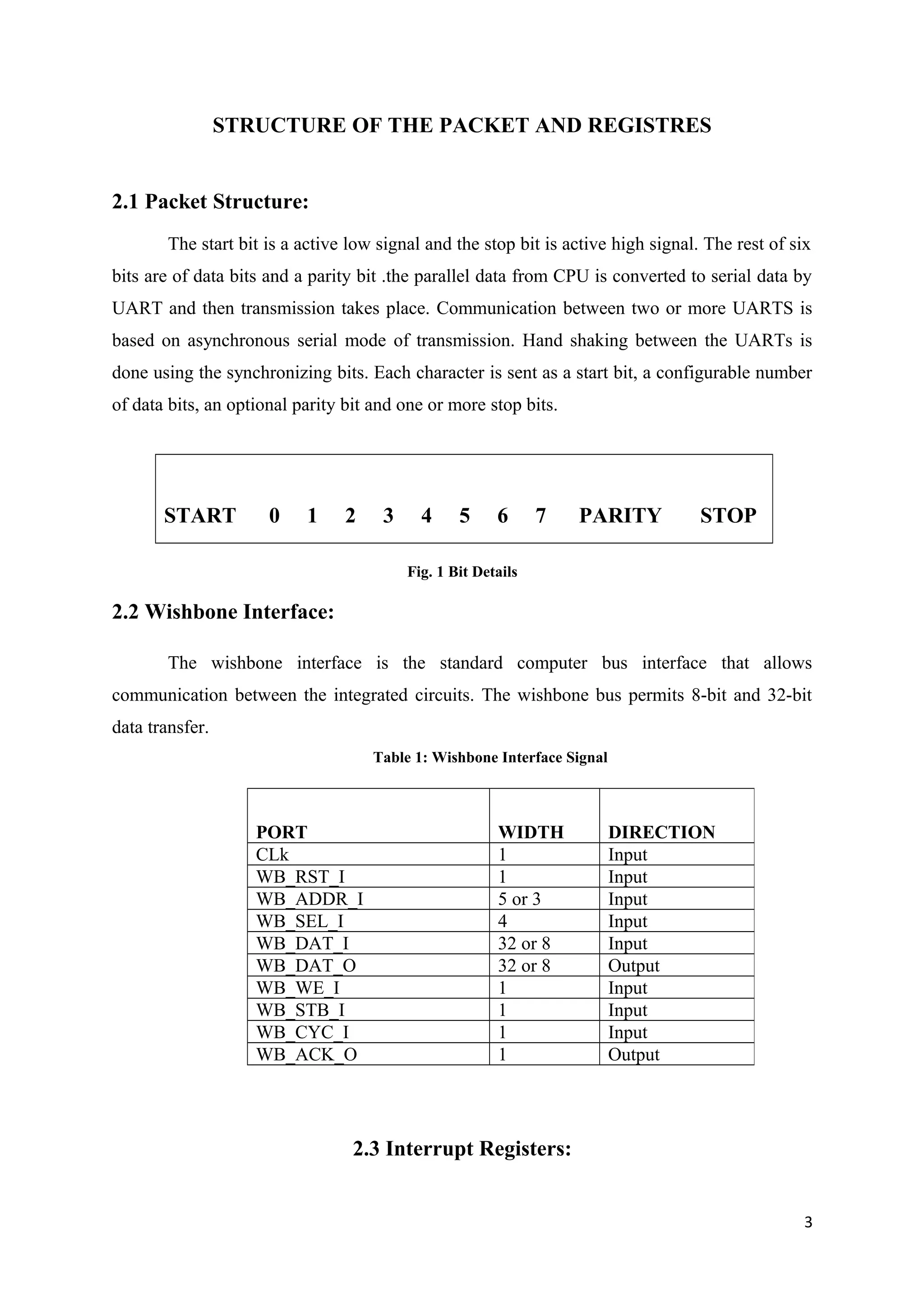
CHAPTER 1
INTRODUCTION
UART Verification IP provides an smart way to verify the UART component of a
SOC or a ASIC. The Universal Asynchronous Receiver Transmitter (UART) is a popular and
widely-used device for data communication in the field of telecommunication. It is frequently
used to implement the serial port for IBM PC compatible personal computers, where it is
often connected to an RS-232 interface for modems, printers, and similar peripherals.
There are different versions of UARTs in the industry. Some of them contain FIFOs
for the receiver/transmitter data buffering and some of them have the 9 data bits mode (start
bit + 8 data bits + parity + stop bits). This reference design describes a fully configurable
UART optimized for and implemented in a variety of Lattice devices, which offer superior
performance and architecture compared to existing semiconductor ASSPs (application-
specific standard products). The receiver performs serial-to-parallel conversion on the
asynchronous data frame received from the serial data input . The transmitter performs
parallel to serial conversion on the 8-bit data received from the CPU. In order to synchronize
the asynchronous serial data and to insure the data integrity, start, parity and stop bits are
added to the serial data.
The UART IP core consists of a transmitter, a receiver, a modem interface, a baud
generator, an interrupt controller, and various control and status registers. This core can
operate in 8-bit data bus mode or in 32-bit bus mode, which is now the default mode. It is an
interface between wishbone compatible UART transceiver, which allows communication
with modem or other external devices, like another computer using a serial cable and RS232
protocol.
The data transmission takes place in between the chips, inside the chips and in
between the systems also. As it is asynchronous clock there will be no methodology to
establish the clock distribution techniques.
There are three of modes in UART. They are
1) HALFDUPLEX MODE: In the half duplex mode either transmission or reception takes
place at a time.
1
2) FULLDUPLEX MODE: In the full duplex mode both transmission and reception takes
place at time.
3) LOOP BACK MODE: It is used for testing purpose. We will be connection the
transmitter and receiver of same UART this helps to check the accuracy of it.
CHAPTER 2
2
STRUCTURE OF THE PACKET AND REGISTRES
2.1 Packet Structure:
The start bit is a active low signal and the stop bit is active high signal. The rest of six
bits are of data bits and a parity bit .the parallel data from CPU is converted to serial data by
UART and then transmission takes place. Communication between two or more UARTS is
based on asynchronous serial mode of transmission. Hand shaking between the UARTs is
done using the synchronizing bits. Each character is sent as a start bit, a configurable number
of data bits, an optional parity bit and one or more stop bits.
START 0 1 2 3 4 5 6 7 PARITY STOP
Fig. 1 Bit Details
2.2 Wishbone Interface:
The wishbone interface is the standard computer bus interface that allows
communication between the integrated circuits. The wishbone bus permits 8-bit and 32-bit
data transfer.
Table 1: Wishbone Interface Signal
2.3 Interrupt Registers:
3
PORT WIDTH DIRECTION
CLk 1 Input
WB_RST_I 1 Input
WB_ADDR_I 5 or 3 Input
WB_SEL_I 4 Input
WB_DAT_I 32 or 8 Input
WB_DAT_O 32 or 8 Output
WB_WE_I 1 Input
WB_STB_I 1 Input
WB_CYC_I 1 Input
WB_ACK_O 1 Output
This register is used to enable and identify the interrupts. There are two types of
interrupt registers. They are
a) Interrupt Enable Register
b) Interrupt Identification Register.
The interrupt enable register enables and disables with interrupt generation by the UART. It
is of 8-bit width. The interrupt identification register enables the programmer to retrieve the
current highest priority pending interrupt. BIT-0 indicates that an interrupt is pending when
its logic 0.when it is 1 the interrupt is not in pending. The width of the register is 8-bit.
2.4 Control Registers:
There are two Control registers. They are
a) FIFO control register
b) LINE control register
The FIFO control register allows selection of the FIFO trigger level. The FIFO register is of
8-bit data width. The 0th bit should be always 0.The line control register allows the
specification of the format of the asynchronous data communication used. A bit in the
register also allows access to the divisor latches, which define the baud rate. Reading from
the register is allowed to check the current setting of the communication.
2.5 Baud Generator:
The baud generator is responsible for generating a periodic baud pulse based on the
divisor latch value which determines the baud rate for the serial transmission. This periodic
pulse is used by transmitter and receiver to generate sampling pulses for sampling both
received data and data to be transmitted. One baud out occurs for sixteen clock cycles. For
sixteen clock cycles one bit data will be sent. There are two debug registers they work in32-
bit data bus mode. It has 5-bit address mode. It is read only and is provided for debugging
purpose for chip testing. Each has a 256-byte FIFO to buffer data flow. The use of FIFO
buffers increases the overall transmission rate by allowing slower processors to respond, and
reducing the amount of time wasted context switching. Besides data transfer, they also
facilitate start/stop framing bits, check various parity options, as well as detect transmission
errors.
2.6 Divisor Latches:
4
The divisor latches can be accessed by setting the 7th bit of LCR to 1.Restore the bit
to zero after setting the divisor latches in order to restore access to the other registers that
occupy the same address. The two bytes form one sixteen bit register, which is internally
accessed as a single number. In order to have normal operation two bytes are driven to zero
on reset. The reset disables all serial I/O operations in order to ensure explicit setup of the
register in the software. The value set should be equal to (system clock speed) / (16 * desired)
baud rate. The internal counter starts to work when the LSB of DL is return, so when setting
the divisor, write the MSB first then LSB last.
CHAPTER 3
BLOCK DIAGRAM
5
SRX_I
Wishbone
Signals
STX_O
INT_O
RTS_O
CTS_I
DTR_O
DSR_I
DCD_I
RI_I
Fig. 2 Block Diagram of the UART core
The UART core consists of a transmitter, a receiver, a modem interface, a baud
generator, an interrupt controller, and various control and status registers. The transmitter and
6
Baud
Generator
Logic
Interrupt
Logic
Modem
Signals
Logic
Transmitter
Shift
Register
Receiver Shift
Register
Transmitter
Logic
Receiver
Logic
Divisor
Latch
Registers
Line Status
Register
Line
Control
Register
Receiver
FIFO
FIFO
Control
Register
Transmitter
FIFO
Interrupt ID
Register
Interrupt
Enable
Register
Modem
Status
Register
Modem
Control
Register
WISHBONE
bus
Interface
receiver perform parallel-to-serial and serial-to-parallel conversions, respectively. Each has a
FIFO to buffer data flow.
The use of FIFO buffers increases the overall transmission rate by allowing slower
processors to respond, and reducing the amount of time wasted on context switching. Besides
data transfer, they also facilitate start/stop framing bits, check various parity options, as well
as detect transmission errors. The modem interface allows the processor to transmit data to
another terminal or handshake to the modem input signals. It also makes the modem's status
available to the processor. The baud generator creates a baud rate clock and a receiver
reference clock. The interrupt controller works with the transmitter, receiver, and modem
interface to notify the processor of events that require intervention. Some examples of these
events are transmission errors and modem status changes. The processor has access to the
complete status of the UART at any time. Information reported includes the line condition,
modem status, as well as any errors such as parity, overrun, framing, or line break. The
processor can also configure the UART's operation via various control registers.
CHAPTER 4
UVM ARCHITECTURE
7
Fig. 3 Block Diagram of UVM Architecture
UVM architecture for UART IP core is as shown in above diagram. It indicates
overall plane for the project as how many and which components are needed for the project
architecture. Along with architecture we also require the verification plane. It is formulating,
architecting, strategizing and documenting an overall verification blueprint.
All required components are discussed below
4.1 Transaction Class:
During verification of this project we have some handshaking signals and some
signals which should act as input to one UART and output to another and vice versa. So in
order to achieve this we made use of two transaction classes for each UART. The class is
extended from uvm_sequence_item. The class is then registered to the factory by using
uvm_object_utils. The signals required for particular UART needs to be declared in the
8
respective transaction classes. And the signals which are to be randomized have to be
declared ‘rand’. The signals are registered to the factory using Macros.
We defined some constraints according to the needs of the project. These constraints
will randomize the data as required in the protocol. The select signal WB_SEL_I is
hardcoded to 1 always. And for writing data to UART’s FIFO WB_WE_I must be high and
for reading from the receiver FIFO the signal should be kept zero. For each data and address,
the strobe and cycle must be made high and after receiving the acknowledgement for the
successful transmission, strobe and cycle must be made low.
4.2 Agent:
It defines whether the sequencer, driver and monitor are to be created or not, using an
enum which is defined in UVM factory i.e. uvm_active_passive_enum. If the value of this
enum is equal to is_active all there sub-blocks i.e. driver, sequencer and monitor are created
but if value is equal to is_passive only monitor is created. This enum can be set from the
testcase. This agent also connects the sequencer and driver during connect phase. In this
project there are two agents i.e. master agent and salve agent, which will create their own
driver, sequencer and monitor,so both are active agents.
4.3 Driver:
The driver as name specified drives the data on to the interface. The driver in UVM is
extended from uvm_driver and parameterized by transaction class. There are two drivers in
our project one for each UART. Both the drivers get the interface using local configuration
db class. In run phase we drive the data according to protocol.
The two drivers for each UART function similarly since UART is a device which
transmits and receives the data simultaneously. So we need to drive both read as well as write
signals from both the drivers.
For the transmission of the data driver initially drives address and data in on to the
interface along with strobe, cycle and write enable signals. As soon as it receives the
9
acknowledgement strobe and cycle must be driven zero. This should be repeated till the
transmission of entire data byte.
Meanwhile the driver should drive the necessary address and data for reading the
data from the UART. For reading data from the UART we need to enable Line status register
and make write enable low, after the LSR’s address is driven and acknowledgement is
received, the strobe and cycle must be made low separately in a loop and when LSR’s LSB
bit goes high, the address for reading the data from the receiver FIFO should be driven with
strobe and cycle signals.
4.4 Sequencer:
The sequencer in UVM just acts as a bridge between sequence and driver. This is the
only non-virtual class in our UVM factory. The sequencer is also parameterized by
transaction class. The sequencer takes the randomized data from sequences and passes it to
the driver to which it is connected. The sequencers for both agents have same functionality
and hence have same code.
4.5 Monitor:
The monitor as name specified monitors the data transferred between two UARTs.
The monitor in UVM is extended from uvm_monitor and parameterized by transaction class.
There are two monitors in our project one for each UART. Both the monitors get the interface
using local configuration db class. In run phase we collect the data according to protocol.
It takes the data from the interface into some local variables and passes it to
scoreboard using transaction class. The monitor and scoreboard are connected using analysis
port and analysis export respectively. These ports are to be declared and then created in
monitor and scoreboard respectively. The connection between them is made in the upper
level where scoreboard is being created i.e. environment. Here monitor collects two data
bytes, one is transmitted data of the same UART and another is received data which is
transmitted by another UART. Collected data packet is sent to scoreboard using analysis
ports.
4.6 Sequence:
10
Firstly we will make a base sequence extending from UVM_sequence and then other
child sequences are made using this base sequence. This class is used to randomize the
transaction class for each UART. Here we are using two sequences which will generate two
transactions one for each UART. In sequences we are overriding the address and data in order
to configure the registers. The sequence randomizes the data based on constraints in
transaction class and inline constraints.
4.7 Test:
Test is a place where we run the sequences. As in sequences here also we have a base
test that will be extended from UVM_test. The further child tests will be made from this base
test class. In base test we will set all the parameters of configuration db class according to our
requirements. We will also get the interface set in top and again set it to the interface handles
in local configuration db classes. The base test also creates the environment. All these things
happen in build phase of base test. In child test we just create the handle of sequence and start
it on some sequencer, before start of sequence an objection is raised and the same objection is
dropped after starting sequence. This raise and drop of objection is done so that one who is
simulating could know when the test bench comes out of the run phase.
4.8 Environment:
This class is created in test and is also a most important component of our test bench.
Environment creates agent-tops, scoreboard, virtual sequencer (if required) etc. The
environment makes connection between monitors and scoreboard. In case one has virtual
sequencer one has to connect physical sequencers with the handles of physical sequencers in
virtual sequencer. Here we also set the local configuration db class parameters.
4.9 Scoreboard:
The scoreboard compares the data sent from one side to another i.e. from one UART
to another and vice-versa. Here we are taking four queues for storing the data collected from
monitors. Two queues store input and output data from one UART and remaining two queues
store the input and output data from another UART. This also includes cover groups which
helps in coverage. It gets the data from both monitors and compares them. Also it samples the
11
signal values which have been covered. We have used $test$plusargs in scoreboard for
checking. Comparison will be made only if string matching happens.
4.10 Virtual Sequencer:
Virtual sequencer is extended from uvm_sequencer and is parameterized by
uvm_sequence_item. This is parameterized by uvm_sequence_item because this sequencer
has to take both type of data. This sequencer is required because we cannot run virtual
sequences on physical sequencers so we make a virtual sequencer and run sequences on it.
This sequencer is pointed to parent type handle of sequencer in virtual sequence using $cast.
The virtual sequencer has the handles of physical sequencers which are pointed to physical
sequencers in the environment.
4.11 Virtual Sequence:
Virtual sequence is also extended from uvm_sequence as normal sequences but is
parameterized by uvm_sequence_item. It has handles of both master and slave sequences
written, handles of physical sequencers and virtual sequencer. This class has a base sequence
which will connect handles of physical sequencers to the handles of physical sequencers in
virtual sequencer. In child sequences one has to create handles of physical sequence which is
to be started and after creating we start it. This virtual sequence handle is made in test and
then it is created and then started. The start from test calls this start and these starts go to
respective physical sequence and start that sequence.
CHAPTER 5
TEST CASES
12
Different test cases are used for verification purpose. Following are some test cases which
used for verification of the design,
1. Half Duplex Mode: For 1, 4, 8 & 14 bytes FIFO trigger level.
2. Full Duplex Mode
3. Loop Back Mode
4. Parity Error
5. Break interrupt
6. Overrun condition
7. Framing Error
8. Timeout Indication
9. Transmitter holding register empty
10. Setting LCR to Transmitting 5 bits data
11. Setting LCR to Transmitting 6 bits data
12. Setting LCR to Transmitting 7 bits data
CHAPTER 6
13
CONCLUSION
The UART IP core working has been verified for different modes of operations i.e.
HALF DUPLEX MODE , FULL DUPLEX MODE and LOOP BACK MODE. Also the
design is verified for different test cases for errors like parity error, overrun error, framing
error, break interrupt. The design is verified successfully with all above test cases.
14

NAVEEN UART BATCH 43

  • 1.
    CHAPTER 1 INTRODUCTION UART VerificationIP provides an smart way to verify the UART component of a SOC or a ASIC. The Universal Asynchronous Receiver Transmitter (UART) is a popular and widely-used device for data communication in the field of telecommunication. It is frequently used to implement the serial port for IBM PC compatible personal computers, where it is often connected to an RS-232 interface for modems, printers, and similar peripherals. There are different versions of UARTs in the industry. Some of them contain FIFOs for the receiver/transmitter data buffering and some of them have the 9 data bits mode (start bit + 8 data bits + parity + stop bits). This reference design describes a fully configurable UART optimized for and implemented in a variety of Lattice devices, which offer superior performance and architecture compared to existing semiconductor ASSPs (application- specific standard products). The receiver performs serial-to-parallel conversion on the asynchronous data frame received from the serial data input . The transmitter performs parallel to serial conversion on the 8-bit data received from the CPU. In order to synchronize the asynchronous serial data and to insure the data integrity, start, parity and stop bits are added to the serial data. The UART IP core consists of a transmitter, a receiver, a modem interface, a baud generator, an interrupt controller, and various control and status registers. This core can operate in 8-bit data bus mode or in 32-bit bus mode, which is now the default mode. It is an interface between wishbone compatible UART transceiver, which allows communication with modem or other external devices, like another computer using a serial cable and RS232 protocol. The data transmission takes place in between the chips, inside the chips and in between the systems also. As it is asynchronous clock there will be no methodology to establish the clock distribution techniques. There are three of modes in UART. They are 1) HALFDUPLEX MODE: In the half duplex mode either transmission or reception takes place at a time. 1
  • 2.
    2) FULLDUPLEX MODE:In the full duplex mode both transmission and reception takes place at time. 3) LOOP BACK MODE: It is used for testing purpose. We will be connection the transmitter and receiver of same UART this helps to check the accuracy of it. CHAPTER 2 2
  • 3.
    STRUCTURE OF THEPACKET AND REGISTRES 2.1 Packet Structure: The start bit is a active low signal and the stop bit is active high signal. The rest of six bits are of data bits and a parity bit .the parallel data from CPU is converted to serial data by UART and then transmission takes place. Communication between two or more UARTS is based on asynchronous serial mode of transmission. Hand shaking between the UARTs is done using the synchronizing bits. Each character is sent as a start bit, a configurable number of data bits, an optional parity bit and one or more stop bits. START 0 1 2 3 4 5 6 7 PARITY STOP Fig. 1 Bit Details 2.2 Wishbone Interface: The wishbone interface is the standard computer bus interface that allows communication between the integrated circuits. The wishbone bus permits 8-bit and 32-bit data transfer. Table 1: Wishbone Interface Signal 2.3 Interrupt Registers: 3 PORT WIDTH DIRECTION CLk 1 Input WB_RST_I 1 Input WB_ADDR_I 5 or 3 Input WB_SEL_I 4 Input WB_DAT_I 32 or 8 Input WB_DAT_O 32 or 8 Output WB_WE_I 1 Input WB_STB_I 1 Input WB_CYC_I 1 Input WB_ACK_O 1 Output
  • 4.
    This register isused to enable and identify the interrupts. There are two types of interrupt registers. They are a) Interrupt Enable Register b) Interrupt Identification Register. The interrupt enable register enables and disables with interrupt generation by the UART. It is of 8-bit width. The interrupt identification register enables the programmer to retrieve the current highest priority pending interrupt. BIT-0 indicates that an interrupt is pending when its logic 0.when it is 1 the interrupt is not in pending. The width of the register is 8-bit. 2.4 Control Registers: There are two Control registers. They are a) FIFO control register b) LINE control register The FIFO control register allows selection of the FIFO trigger level. The FIFO register is of 8-bit data width. The 0th bit should be always 0.The line control register allows the specification of the format of the asynchronous data communication used. A bit in the register also allows access to the divisor latches, which define the baud rate. Reading from the register is allowed to check the current setting of the communication. 2.5 Baud Generator: The baud generator is responsible for generating a periodic baud pulse based on the divisor latch value which determines the baud rate for the serial transmission. This periodic pulse is used by transmitter and receiver to generate sampling pulses for sampling both received data and data to be transmitted. One baud out occurs for sixteen clock cycles. For sixteen clock cycles one bit data will be sent. There are two debug registers they work in32- bit data bus mode. It has 5-bit address mode. It is read only and is provided for debugging purpose for chip testing. Each has a 256-byte FIFO to buffer data flow. The use of FIFO buffers increases the overall transmission rate by allowing slower processors to respond, and reducing the amount of time wasted context switching. Besides data transfer, they also facilitate start/stop framing bits, check various parity options, as well as detect transmission errors. 2.6 Divisor Latches: 4
  • 5.
    The divisor latchescan be accessed by setting the 7th bit of LCR to 1.Restore the bit to zero after setting the divisor latches in order to restore access to the other registers that occupy the same address. The two bytes form one sixteen bit register, which is internally accessed as a single number. In order to have normal operation two bytes are driven to zero on reset. The reset disables all serial I/O operations in order to ensure explicit setup of the register in the software. The value set should be equal to (system clock speed) / (16 * desired) baud rate. The internal counter starts to work when the LSB of DL is return, so when setting the divisor, write the MSB first then LSB last. CHAPTER 3 BLOCK DIAGRAM 5
  • 6.
    SRX_I Wishbone Signals STX_O INT_O RTS_O CTS_I DTR_O DSR_I DCD_I RI_I Fig. 2 BlockDiagram of the UART core The UART core consists of a transmitter, a receiver, a modem interface, a baud generator, an interrupt controller, and various control and status registers. The transmitter and 6 Baud Generator Logic Interrupt Logic Modem Signals Logic Transmitter Shift Register Receiver Shift Register Transmitter Logic Receiver Logic Divisor Latch Registers Line Status Register Line Control Register Receiver FIFO FIFO Control Register Transmitter FIFO Interrupt ID Register Interrupt Enable Register Modem Status Register Modem Control Register WISHBONE bus Interface
  • 7.
    receiver perform parallel-to-serialand serial-to-parallel conversions, respectively. Each has a FIFO to buffer data flow. The use of FIFO buffers increases the overall transmission rate by allowing slower processors to respond, and reducing the amount of time wasted on context switching. Besides data transfer, they also facilitate start/stop framing bits, check various parity options, as well as detect transmission errors. The modem interface allows the processor to transmit data to another terminal or handshake to the modem input signals. It also makes the modem's status available to the processor. The baud generator creates a baud rate clock and a receiver reference clock. The interrupt controller works with the transmitter, receiver, and modem interface to notify the processor of events that require intervention. Some examples of these events are transmission errors and modem status changes. The processor has access to the complete status of the UART at any time. Information reported includes the line condition, modem status, as well as any errors such as parity, overrun, framing, or line break. The processor can also configure the UART's operation via various control registers. CHAPTER 4 UVM ARCHITECTURE 7
  • 8.
    Fig. 3 BlockDiagram of UVM Architecture UVM architecture for UART IP core is as shown in above diagram. It indicates overall plane for the project as how many and which components are needed for the project architecture. Along with architecture we also require the verification plane. It is formulating, architecting, strategizing and documenting an overall verification blueprint. All required components are discussed below 4.1 Transaction Class: During verification of this project we have some handshaking signals and some signals which should act as input to one UART and output to another and vice versa. So in order to achieve this we made use of two transaction classes for each UART. The class is extended from uvm_sequence_item. The class is then registered to the factory by using uvm_object_utils. The signals required for particular UART needs to be declared in the 8
  • 9.
    respective transaction classes.And the signals which are to be randomized have to be declared ‘rand’. The signals are registered to the factory using Macros. We defined some constraints according to the needs of the project. These constraints will randomize the data as required in the protocol. The select signal WB_SEL_I is hardcoded to 1 always. And for writing data to UART’s FIFO WB_WE_I must be high and for reading from the receiver FIFO the signal should be kept zero. For each data and address, the strobe and cycle must be made high and after receiving the acknowledgement for the successful transmission, strobe and cycle must be made low. 4.2 Agent: It defines whether the sequencer, driver and monitor are to be created or not, using an enum which is defined in UVM factory i.e. uvm_active_passive_enum. If the value of this enum is equal to is_active all there sub-blocks i.e. driver, sequencer and monitor are created but if value is equal to is_passive only monitor is created. This enum can be set from the testcase. This agent also connects the sequencer and driver during connect phase. In this project there are two agents i.e. master agent and salve agent, which will create their own driver, sequencer and monitor,so both are active agents. 4.3 Driver: The driver as name specified drives the data on to the interface. The driver in UVM is extended from uvm_driver and parameterized by transaction class. There are two drivers in our project one for each UART. Both the drivers get the interface using local configuration db class. In run phase we drive the data according to protocol. The two drivers for each UART function similarly since UART is a device which transmits and receives the data simultaneously. So we need to drive both read as well as write signals from both the drivers. For the transmission of the data driver initially drives address and data in on to the interface along with strobe, cycle and write enable signals. As soon as it receives the 9
  • 10.
    acknowledgement strobe andcycle must be driven zero. This should be repeated till the transmission of entire data byte. Meanwhile the driver should drive the necessary address and data for reading the data from the UART. For reading data from the UART we need to enable Line status register and make write enable low, after the LSR’s address is driven and acknowledgement is received, the strobe and cycle must be made low separately in a loop and when LSR’s LSB bit goes high, the address for reading the data from the receiver FIFO should be driven with strobe and cycle signals. 4.4 Sequencer: The sequencer in UVM just acts as a bridge between sequence and driver. This is the only non-virtual class in our UVM factory. The sequencer is also parameterized by transaction class. The sequencer takes the randomized data from sequences and passes it to the driver to which it is connected. The sequencers for both agents have same functionality and hence have same code. 4.5 Monitor: The monitor as name specified monitors the data transferred between two UARTs. The monitor in UVM is extended from uvm_monitor and parameterized by transaction class. There are two monitors in our project one for each UART. Both the monitors get the interface using local configuration db class. In run phase we collect the data according to protocol. It takes the data from the interface into some local variables and passes it to scoreboard using transaction class. The monitor and scoreboard are connected using analysis port and analysis export respectively. These ports are to be declared and then created in monitor and scoreboard respectively. The connection between them is made in the upper level where scoreboard is being created i.e. environment. Here monitor collects two data bytes, one is transmitted data of the same UART and another is received data which is transmitted by another UART. Collected data packet is sent to scoreboard using analysis ports. 4.6 Sequence: 10
  • 11.
    Firstly we willmake a base sequence extending from UVM_sequence and then other child sequences are made using this base sequence. This class is used to randomize the transaction class for each UART. Here we are using two sequences which will generate two transactions one for each UART. In sequences we are overriding the address and data in order to configure the registers. The sequence randomizes the data based on constraints in transaction class and inline constraints. 4.7 Test: Test is a place where we run the sequences. As in sequences here also we have a base test that will be extended from UVM_test. The further child tests will be made from this base test class. In base test we will set all the parameters of configuration db class according to our requirements. We will also get the interface set in top and again set it to the interface handles in local configuration db classes. The base test also creates the environment. All these things happen in build phase of base test. In child test we just create the handle of sequence and start it on some sequencer, before start of sequence an objection is raised and the same objection is dropped after starting sequence. This raise and drop of objection is done so that one who is simulating could know when the test bench comes out of the run phase. 4.8 Environment: This class is created in test and is also a most important component of our test bench. Environment creates agent-tops, scoreboard, virtual sequencer (if required) etc. The environment makes connection between monitors and scoreboard. In case one has virtual sequencer one has to connect physical sequencers with the handles of physical sequencers in virtual sequencer. Here we also set the local configuration db class parameters. 4.9 Scoreboard: The scoreboard compares the data sent from one side to another i.e. from one UART to another and vice-versa. Here we are taking four queues for storing the data collected from monitors. Two queues store input and output data from one UART and remaining two queues store the input and output data from another UART. This also includes cover groups which helps in coverage. It gets the data from both monitors and compares them. Also it samples the 11
  • 12.
    signal values whichhave been covered. We have used $test$plusargs in scoreboard for checking. Comparison will be made only if string matching happens. 4.10 Virtual Sequencer: Virtual sequencer is extended from uvm_sequencer and is parameterized by uvm_sequence_item. This is parameterized by uvm_sequence_item because this sequencer has to take both type of data. This sequencer is required because we cannot run virtual sequences on physical sequencers so we make a virtual sequencer and run sequences on it. This sequencer is pointed to parent type handle of sequencer in virtual sequence using $cast. The virtual sequencer has the handles of physical sequencers which are pointed to physical sequencers in the environment. 4.11 Virtual Sequence: Virtual sequence is also extended from uvm_sequence as normal sequences but is parameterized by uvm_sequence_item. It has handles of both master and slave sequences written, handles of physical sequencers and virtual sequencer. This class has a base sequence which will connect handles of physical sequencers to the handles of physical sequencers in virtual sequencer. In child sequences one has to create handles of physical sequence which is to be started and after creating we start it. This virtual sequence handle is made in test and then it is created and then started. The start from test calls this start and these starts go to respective physical sequence and start that sequence. CHAPTER 5 TEST CASES 12
  • 13.
    Different test casesare used for verification purpose. Following are some test cases which used for verification of the design, 1. Half Duplex Mode: For 1, 4, 8 & 14 bytes FIFO trigger level. 2. Full Duplex Mode 3. Loop Back Mode 4. Parity Error 5. Break interrupt 6. Overrun condition 7. Framing Error 8. Timeout Indication 9. Transmitter holding register empty 10. Setting LCR to Transmitting 5 bits data 11. Setting LCR to Transmitting 6 bits data 12. Setting LCR to Transmitting 7 bits data CHAPTER 6 13
  • 14.
    CONCLUSION The UART IPcore working has been verified for different modes of operations i.e. HALF DUPLEX MODE , FULL DUPLEX MODE and LOOP BACK MODE. Also the design is verified for different test cases for errors like parity error, overrun error, framing error, break interrupt. The design is verified successfully with all above test cases. 14