Downloaded 346 times


![2013-5-13 20
Step-1. Function Kernighan-Lin (G(V,E))
Step-2. Determine a balanced initial Partition of The Nodes
into Sets A and B
Step-3. do
Step-4. A1 := A; B1 := B
Step-5. Compute D Values For All a in A1 and b in B1
Step-6. For (i := 1 to |V|/2)
Step-7. Find a[i] From A1 and b[i] From B1, Such That
g[i] = D[a[i]] + D[b[i]] - 2*c[a[i]][b[i]] is Maximal
Step-8. Move a[i] to B1 and b[i] to A1
www.i-world-tech.blogspot.in](https://image.slidesharecdn.com/vlsiphysicaldesign-130513191024-phpapp01/85/Vlsi-physical-design-20-320.jpg)
![2013-5-13 21
Step-9. Remove a[i] and b[i] From Further Consideration in
This Pass
Step-10. Update D Values For The Elements of A1 = A1 /
a[i] and B1 = B1 / b[i]
Step-11. End for
Step-12. Find k Which Maximizes g_max, The Sum of
g[1],...,g[k]
Step-13. if (g_max > 0) Then
Step-14. Exchange a[1],a[2],...,a[k] With b[1],b[2],...,b[k]
Step-15. Until (g_max <= 0)
Step-16. Return G(V,E)
www.i-world-tech.blogspot.in](https://image.slidesharecdn.com/vlsiphysicaldesign-130513191024-phpapp01/85/Vlsi-physical-design-21-320.jpg)


![2013-5-13 35www.i-world-tech.blogspot.in
Problem : Given a Set of Segments (intervals) [ximin , ximax], Put non-Overlapping
Segments on The Same Track Such That The Number of Tracks is Minimal.](https://image.slidesharecdn.com/vlsiphysicaldesign-130513191024-phpapp01/85/Vlsi-physical-design-35-320.jpg)


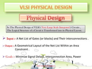
The document discusses the physical design process for VLSI circuits. It describes the main steps as partitioning, floor planning and placement, routing, layout optimization, and extraction and verification. The goals of physical design are to minimize signal delays, interconnection area, and power usage. Physical design transforms the logical structure of a circuit into its physical layout.