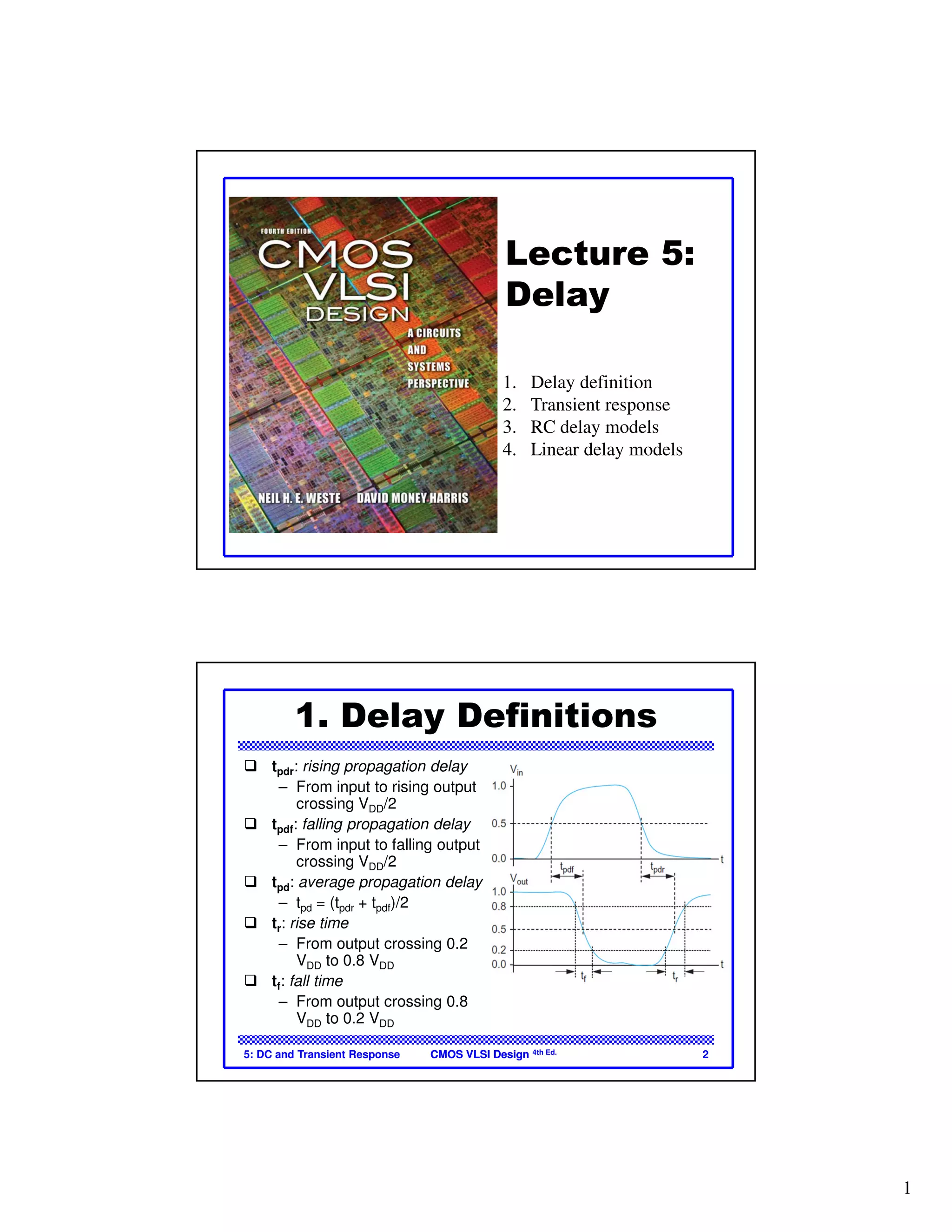
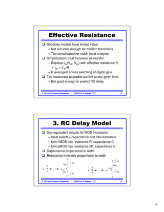
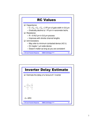
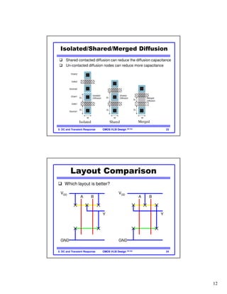
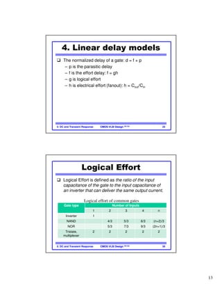
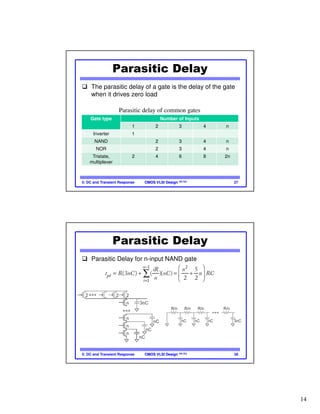
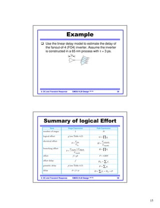
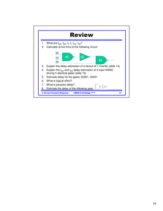
TataKelola dan KamSiber Kecerdasan Buatan v022.pdf
2016 ch4 delay
1. 1
Lecture 5:
Delay
1. Delay definition
2. Transient response
3. RC delay models
4. Linear delay models
CMOS VLSI DesignCMOS VLSI Design 4th Ed.5: DC and Transient Response 2
1. Delay Definitions
tpdr: rising propagation delay
– From input to rising output
crossing VDD/2
tpdf: falling propagation delay
– From input to falling output
crossing VDD/2
tpd: average propagation delay
– tpd = (tpdr + tpdf)/2
tr: rise time
– From output crossing 0.2
VDD to 0.8 VDD
tf: fall time
– From output crossing 0.8
VDD to 0.2 VDD
2. 2
CMOS VLSI DesignCMOS VLSI Design 4th Ed.5: DC and Transient Response 3
1. Delay Definitions
tcdr: rising contamination delay
– From input to rising output crossing VDD/2
tcdf: falling contamination delay
– From input to falling output crossing VDD/2
tcd: average contamination delay
– tpd = (tcdr + tcdf)/2
CMOS VLSI DesignCMOS VLSI Design 4th Ed.
Arrival time
Arrival time is the latest time at which each node in a block of logic
will switch
The slack is the difference between the required and arrival times.
Positive slack means that the circuit meets timing.
Negative slack means that the circuit is not fast enough.
5: DC and Transient Response 4
3. 3
CMOS VLSI DesignCMOS VLSI Design 4th Ed.5: DC and Transient Response 5
2. Transient Response
DC analysis tells us Vout if Vin is constant
Transient analysis tells us Vout(t) if Vin(t) changes
– Requires solving differential equations
Input is usually considered to be a step or ramp
– From 0 to VDD or vice versa
CMOS VLSI DesignCMOS VLSI Design 4th Ed.5: DC and Transient Response 6
DC Response
DC Response: Vout vs. Vin for a gate
Ex: Inverter
– When Vin = 0 -> Vout = VDD
– When Vin = VDD -> Vout = 0
– In between, Vout depends on
transistor size and current
– By KCL, must settle such that
Idsn = |Idsp|
– We could solve equations
– But graphical solution gives more insight
Idsn
Idsp
Vout
VDD
Vin
4. 4
CMOS VLSI DesignCMOS VLSI Design 4th Ed.5: DC and Transient Response 7
Transistor Operation
Current depends on region of transistor behavior
For what Vin and Vout are nMOS and pMOS in
– Cutoff?
– Linear?
– Saturation?
CMOS VLSI DesignCMOS VLSI Design 4th Ed.5: DC and Transient Response 8
Inverter Step Response
Ex: find step response of inverter driving load cap
0
0
( )
( )
( )
(
(
)
)
DD
DD
loa
d
ou
i
d
t
o
n
ut sn
V
V
u t t V
t t
V t
V
d
dt C
t
I t
= −
=
= −
<
( )
0
2
2
0
2
)
)
(
( )
( DD DD t
DD
out
out
out out D t
n
t
ds
D
I V
t t
V V V V
V V V VV
t
V t
V t
β
β
≤
= − > −
− − < −
Vout(t)
Vin(t)
t0
t
Vin
(t)
Vout
(t)
Cload
Idsn
(t)
5. 5
CMOS VLSI DesignCMOS VLSI Design 4th Ed.5: DC and Transient Response 9
Simulated Inverter Delay
Solving differential equations by hand is too hard
SPICE simulator solves the equations numerically
– Uses more accurate I-V models too!
But simulations take time to write, may hide insight
(V)
0.0
0.5
1.0
1.5
2.0
t(s)
0.0 200p 400p 600p 800p 1n
tpdf
= 66ps tpdr
= 83ps
Vin
Vout
CMOS VLSI DesignCMOS VLSI Design 4th Ed.5: DC and Transient Response 10
Delay Estimation
We would like to be able to easily estimate delay
– Not as accurate as simulation
– But easier to ask “What if?”
The step response usually looks like a 1st order RC
response with a decaying exponential.
Use RC delay models to estimate delay
– C = total capacitance on output node
– Use effective resistance R
– So that tpd = RC
Characterize transistors by finding their effective R
– Depends on average current as gate switches
6. 6
CMOS VLSI DesignCMOS VLSI Design 4th Ed.5: DC and Transient Response 11
Effective Resistance
Shockley models have limited value
– Not accurate enough for modern transistors
– Too complicated for much hand analysis
Simplification: treat transistor as resistor
– Replace Ids(Vds, Vgs) with effective resistance R
• Ids = Vds/R
– R averaged across switching of digital gate
Too inaccurate to predict current at any given time
– But good enough to predict RC delay
CMOS VLSI DesignCMOS VLSI Design 4th Ed.5: DC and Transient Response 12
3. RC Delay Model
Use equivalent circuits for MOS transistors
– Ideal switch + capacitance and ON resistance
– Unit nMOS has resistance R, capacitance C
– Unit pMOS has resistance 2R, capacitance C
Capacitance proportional to width
Resistance inversely proportional to width
kg
s
d
g
s
d
kC
kC
kC
R/k
kg
s
d
g
s
d
kC
kC
kC
2R/k
7. 7
CMOS VLSI DesignCMOS VLSI Design 4th Ed.5: DC and Transient Response 13
RC Values
Capacitance
– C = Cg = Cs = Cd = 2 fF/µm of gate width in 0.6 µm
– Gradually decline to 1 fF/µm in nanometer techs.
Resistance
– R ≈ 6 KΩ*µm in 0.6 µm process
– Improves with shorter channel lengths
Unit transistors
– May refer to minimum contacted device (4/2 λ)
– Or maybe 1 µm wide device
– Doesn’t matter as long as you are consistent
CMOS VLSI DesignCMOS VLSI Design 4th Ed.5: DC and Transient Response 14
Inverter Delay Estimate
Estimate the delay of a fanout-of-1 inverter
C
C
R
2C
2C
R
2
1
A
Y
C
2C
C
2C
C
2C
R
Y
2
1
d = 6RC
8. 8
CMOS VLSI DesignCMOS VLSI Design 4th Ed.5: DC and Transient Response 15
Delay Model Comparison
CMOS VLSI DesignCMOS VLSI Design 4th Ed.5: DC and Transient Response 16
Example: 3-input NAND
Sketch a 3-input NAND with transistor widths chosen to
achieve effective rise and fall resistances equal to a unit
inverter (R).
3
3
3
2 2 2
9. 9
CMOS VLSI DesignCMOS VLSI Design 4th Ed.5: DC and Transient Response 17
2 2 2
3
3
3
3C
3C
3C
3C
2C
2C
2C
2C
2C
2C
3C
3C
3C
2C 2C 2C
3-input NAND Caps
Annotate the 3-input NAND gate with gate and diffusion
capacitance.
CMOS VLSI DesignCMOS VLSI Design 4th Ed.5: DC and Transient Response 18
Elmore Delay
ON transistors look like resistors
Pullup or pulldown network modeled as RC ladder
Elmore delay of RC ladder
R1 R2 R3 RN
C1 C2 C3 CN
( ) ( )
nodes
1 1 1 2 2 1 2... ...
pd i to source i
i
N N
t R C
R C R R C R R R C
− −≈
= + + + + + + +
∑
10. 10
CMOS VLSI DesignCMOS VLSI Design 4th Ed.5: DC and Transient Response 19
Example: 3-input NAND
Estimate worst-case rising and falling delay of 3-input NAND
driving h identical gates.
9C
3C
3C3
3
3
222
5hC
Y
n2
n1
( )9 5pdrt h RC= +
( )( ) ( )( ) ( ) ( )
( )
3 3 3 3 3 3
3 3 9 5
11 5
R R R R R R
pdft C C h C
h RC
= + + + + + +
= +
CMOS VLSI DesignCMOS VLSI Design 4th Ed.5: DC and Transient Response 20
Delay Components
Delay has two parts
– Parasitic delay
• 9 or 11 RC
• Independent of load
– Effort delay
• 5h RC
• Proportional to load capacitance
11. 11
CMOS VLSI DesignCMOS VLSI Design 4th Ed.5: DC and Transient Response 21
Contamination Delay
Best-case (contamination) delay can be substantially less than
propagation delay.
Ex: If all three inputs fall simultaneously
( )
5
9 5 3
3 3
cdr
R
t h C h RC
= + = +
9C
3C
3C3
3
3
222
5hC
Y
n2
n1
CMOS VLSI DesignCMOS VLSI Design 4th Ed.5: DC and Transient Response 22
7C
3C
3C3
3
3
222
3C
2C2C
3C3C
Isolated
Contacted
DiffusionMerged
Uncontacted
Diffusion
Shared
Contacted
Diffusion
Diffusion Capacitance
We assumed contacted diffusion on every s / d.
Good layout minimizes diffusion area
Ex: NAND3 layout shares one diffusion contact
– Reduces output capacitance by 2C
– Merged uncontacted diffusion might help too
12. 12
CMOS VLSI DesignCMOS VLSI Design 4th Ed.
Isolated/Shared/Merged Diffusion
Shared contacted diffusion can reduce the diffusion capacitance
Un-contacted diffusion nodes can reduce more capacitance
5: DC and Transient Response 23
Isolated Shared Merged
CMOS VLSI DesignCMOS VLSI Design 4th Ed.5: DC and Transient Response 24
Layout Comparison
Which layout is better?
A
VDD
GND
B
Y
A
VDD
GND
B
Y
13. 13
CMOS VLSI DesignCMOS VLSI Design 4th Ed.
4. Linear delay models
The normalized delay of a gate: d = f + p
– p is the parasitic delay
– f is the effort delay: f = gh
– g is logical effort
– h is electrical effort (fanout): h = Cout/Cin
5: DC and Transient Response 25
CMOS VLSI DesignCMOS VLSI Design 4th Ed.
Logical Effort
Logical Effort is defined as the ratio of the input
capacitance of the gate to the input capacitance of
an inverter that can deliver the same output current.
5: DC and Transient Response 26
Gate type Number of Inputs
1 2 3 4 n
Inverter 1
NAND 4/3 5/3 6/3 (n+2)/3
NOR 5/3 7/3 9/3 (2n+1)/3
Tristate,
multiplexer
2 2 2 2 2
Logical effort of common gates
14. 14
CMOS VLSI DesignCMOS VLSI Design 4th Ed.
Parasitic Delay
The parasitic delay of a gate is the delay of the gate
when it drives zero load
5: DC and Transient Response 27
Gate type Number of Inputs
1 2 3 4 n
Inverter 1
NAND 2 3 4 n
NOR 2 3 4 n
Tristate,
multiplexer
2 4 6 8 2n
Parasitic delay of common gates
CMOS VLSI DesignCMOS VLSI Design 4th Ed.
Parasitic Delay
Parasitic Delay for n-input NAND gate
5: DC and Transient Response 28
15. 15
CMOS VLSI DesignCMOS VLSI Design 4th Ed.
Example
Use the linear delay model to estimate the delay of
the fanout-of-4 (FO4) inverter. Assume the inverter
is constructed in a 65 nm process with τ = 3 ps.
5: DC and Transient Response 29
CMOS VLSI DesignCMOS VLSI Design 4th Ed.
Summary of logical Effort
5: DC and Transient Response 30
16. 16
CMOS VLSI DesignCMOS VLSI Design 4th Ed.
Review
1. What are tpdr, tpdf, tf, tr, tcdr, tcdf?
2. Calculate arrive time of the following circuit:
3. Explain the delay estimation of a fanout-of-1 inverter (slide 14)
4. Explain the tpdr and tpdf delay estimation of 3-input NAND
driving h identical gates (slide 19).
5. Estimate delay for the gates: AOI21, OAI31
6. What is logical effort?
7. What is parasitic delay?
8. Estimate the delay of the following gate:
5: DC and Transient Response 31
40 3010
20
4030