The document discusses the concept of logical effort in CMOS VLSI design, presenting a method for optimizing circuit topology, gate sizes, and stages to achieve minimal delay. It explains how to compute logical effort, electrical effort, and parasitic delays while providing examples and formulas for practical applications like designing a decoder for a register file. Additionally, it emphasizes the significance of choosing the appropriate number of stages in multistage logic networks for optimal performance.
![CMOS VLSI Design
CMOS VLSI Design 4th Ed.
6: Logical Effort 4
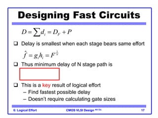
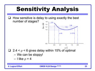
Example
Ben Bitdiddle is the memory designer for the Motoroil 68W86,
an embedded automotive processor. Help Ben design the
decoder for a register file.
Decoder specifications:
– 16 word register file
– Each word is 32 bits wide
– Each bit presents load of 3 unit-sized transistors
– True and complementary address inputs A[3:0]
– Each input may drive 10 unit-sized transistors
Ben needs to decide:
– How many stages to use?
– How large should each gate be?
– How fast can decoder operate?
A[3:0] A[3:0]
16
32 bits
16
words
4:16
Decoder
Register File](https://image.slidesharecdn.com/lecture8-220717085249-897aa5ba/85/Lecture-8-ppt-4-320.jpg)

![CMOS VLSI Design
CMOS VLSI Design 4th Ed.
6: Logical Effort 26
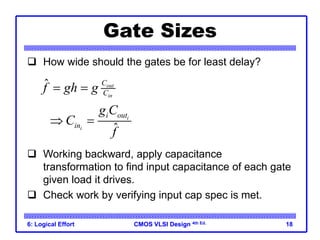
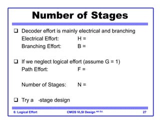
Example, Revisited
Ben Bitdiddle is the memory designer for the Motoroil 68W86,
an embedded automotive processor. Help Ben design the
decoder for a register file.
Decoder specifications:
– 16 word register file
– Each word is 32 bits wide
– Each bit presents load of 3 unit-sized transistors
– True and complementary address inputs A[3:0]
– Each input may drive 10 unit-sized transistors
Ben needs to decide:
– How many stages to use?
– How large should each gate be?
– How fast can decoder operate?
A[3:0] A[3:0]
16
32 bits
16
words
4:16
Decoder
Register File](https://image.slidesharecdn.com/lecture8-220717085249-897aa5ba/85/Lecture-8-ppt-26-320.jpg)
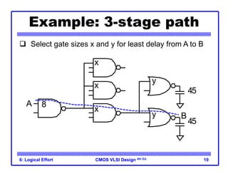
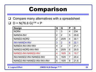
![CMOS VLSI Design
CMOS VLSI Design 4th Ed.
6: Logical Effort 28
Gate Sizes & Delay
Logical Effort: G = 1 * 6/3 * 1 = 2
Path Effort: F = GBH = 154
Stage Effort:
Path Delay:
Gate sizes: z = 96*1/5.36 = 18 y = 18*2/5.36 = 6.7
A[3] A[3] A[2] A[2] A[1] A[1] A[0] A[0]
word[0]
word[15]
96 units of wordline capacitance
10 10 10 10 10 10 10 10
y z
y z
1/3
ˆ 5.36
f F
ˆ
3 1 4 1 22.1
D f
](https://image.slidesharecdn.com/lecture8-220717085249-897aa5ba/85/Lecture-8-ppt-28-320.jpg)


![RF Circuit Design - [Ch1-2] Transmission Line Theory](https://cdn.slidesharecdn.com/ss_thumbnails/ch1-2-150613064349-lva1-app6892-thumbnail.jpg?width=640&height=640&fit=bounds)