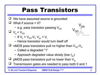
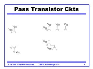
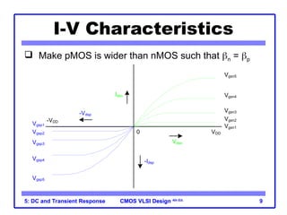
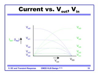
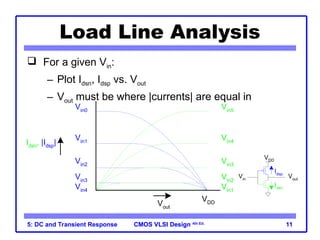
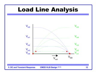
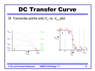
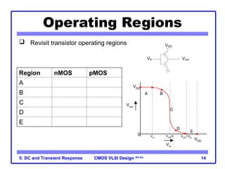
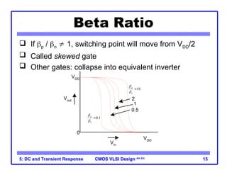
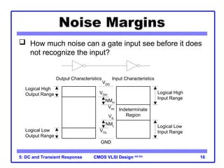
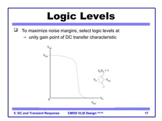
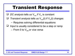
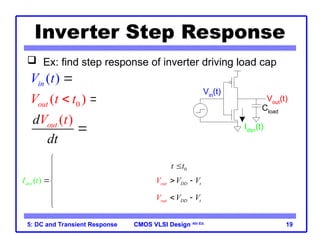
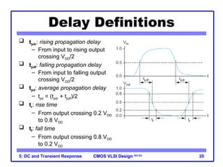
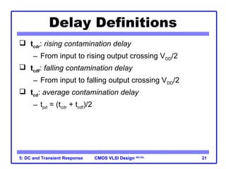
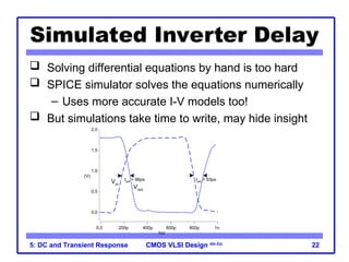
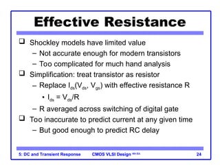
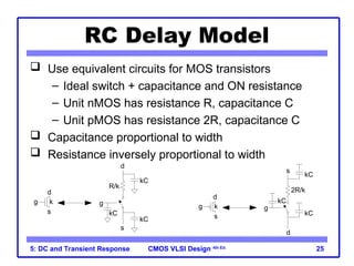
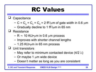
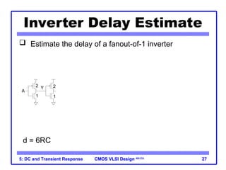
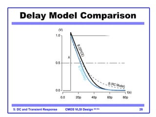
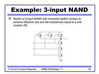
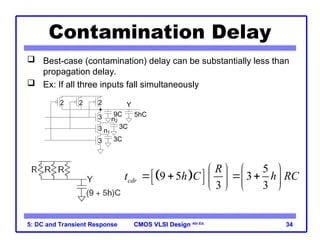
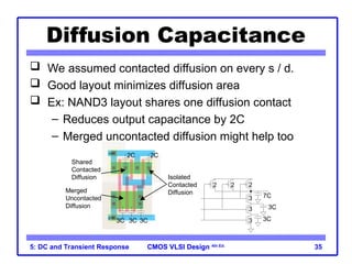
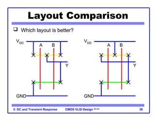
Lecture 5:
DC &
Transient
Response
CMOS VLSI Design
CMOS VLSI Design 4th Ed.
5: DC and Transient Response 2
Outline
 Pass Transistors
 DC Response
 Logic Levels and Noise Margins
 Transient Response
 RC Delay Models
 Delay Estimation
CMOS VLSI Design
CMOS VLSI Design 4th Ed.
5: DC and Transient Response 3
Pass Transistors
 We have assumed source is grounded
 What if source > 0?
– e.g. pass transistor passing VDD
 Vg = VDD
– If Vs > VDD-Vt, Vgs < Vt
– Hence transistor would turn itself off
 nMOS pass transistors pull no higher than VDD-Vtn
– Called a degraded “1”
– Approach degraded value slowly (low Ids)
 pMOS pass transistors pull no lower than Vtp
 Transmission gates are needed to pass both 0 and 1
VDD
VDD
CMOS VLSI Design
CMOS VLSI Design 4th Ed.
5: DC and Transient Response 4
Pass Transistor Ckts
VDD
VDD
Vs = VDD-Vtn
VSS
Vs = |Vtp|
VDD
VDD-Vtn VDD-Vtn
VDD-Vtn
VDD
VDD VDD VDD
VDD
VDD-Vtn
VDD-2Vtn
CMOS VLSI Design
CMOS VLSI Design 4th Ed.
5: DC and Transient Response 5
DC Response
 DC Response: Vout vs. Vin for a gate
 Ex: Inverter
– When Vin = 0 -> Vout = VDD
– When Vin = VDD -> Vout = 0
– In between, Vout depends on
transistor size and current
– By KCL, must settle such that
Idsn = |Idsp|
– We could solve equations
– But graphical solution gives more insight
Idsn
Idsp
Vout
VDD
Vin
CMOS VLSI Design
CMOS VLSI Design 4th Ed.
5: DC and Transient Response 6
Transistor Operation
 Current depends on region of transistor behavior
 For what Vin and Vout are nMOS and pMOS in
– Cutoff?
– Linear?
– Saturation?
CMOS VLSI Design
CMOS VLSI Design 4th Ed.
5: DC and Transient Response 7
nMOS Operation
Cutoff Linear Saturated
Vgsn < Vtn
Vin < Vtn
Vgsn > Vtn
Vin > Vtn
Vdsn < Vgsn – Vtn
Vout < Vin - Vtn
Vgsn > Vtn
Vin > Vtn
Vdsn > Vgsn – Vtn
Vout > Vin - Vtn
Idsn
Idsp
Vout
VDD
Vin
Vgsn = Vin
Vdsn = Vout
CMOS VLSI Design
CMOS VLSI Design 4th Ed.
5: DC and Transient Response 8
pMOS Operation
Cutoff Linear Saturated
Vgsp > Vtp
Vin > VDD + Vtp
Vgsp < Vtp
Vin < VDD + Vtp
Vdsp > Vgsp – Vtp
Vout > Vin - Vtp
Vgsp < Vtp
Vin < VDD + Vtp
Vdsp < Vgsp – Vtp
Vout < Vin - Vtp
Idsn
Idsp
Vout
VDD
Vin
Vgsp = Vin - VDD
Vdsp = Vout - VDD
Vtp < 0
CMOS VLSI Design
CMOS VLSI Design 4th Ed.
5: DC and Transient Response 9
I-V Characteristics
 Make pMOS is wider than nMOS such that n = p
Vgsn5
Vgsn4
Vgsn3
Vgsn2
Vgsn1
Vgsp5
Vgsp4
Vgsp3
Vgsp2
Vgsp1
VDD
-VDD
Vdsn
-Vdsp
-Idsp
Idsn
0
CMOS VLSI Design
CMOS VLSI Design 4th Ed.
5: DC and Transient Response 10
Current vs. Vout, Vin
Vin5
Vin4
Vin3
Vin2
Vin1
Vin0
Vin1
Vin2
Vin3
Vin4
Idsn, |Idsp|
Vout
VDD
CMOS VLSI Design
CMOS VLSI Design 4th Ed.
5: DC and Transient Response 11
Load Line Analysis
Vin5
Vin4
Vin3
Vin2
Vin1
Vin0
Vin1
Vin2
Vin3
Vin4
Idsn, |Idsp|
Vout
VDD
 For a given Vin:
– Plot Idsn, Idsp vs. Vout
– Vout must be where |currents| are equal in
Idsn
Idsp
Vout
VDD
Vin
CMOS VLSI Design
CMOS VLSI Design 4th Ed.
5: DC and Transient Response 12
Load Line Analysis
 Vin = 0
Vin0
Vin0
Idsn, |Idsp|
Vout
VDD
Vin1
Vin1
Idsn, |Idsp|
Vout
VDD
Vin2
Vin2
Idsn, |Idsp|
Vout
VDD
Vin3
Vin3
Idsn, |Idsp|
Vout
VDD
Vin4
Vin4
Idsn, |Idsp|
Vout
VDD
Vin5
Idsn, |Idsp|
Vout
VDD
Vin5
Vin4
Vin3
Vin2
Vin1
Vin0
Vin1
Vin2
Vin3
Vin4
Vout
VDD
 Vin = 0
0.2VDD
0.4VDD
0.6VDD
0.8VDD
VDD
CMOS VLSI Design
CMOS VLSI Design 4th Ed.
5: DC and Transient Response 13
DC Transfer Curve
 Transcribe points onto Vin vs. Vout plot
Vin5
Vin4
Vin3
Vin2
Vin1
Vin0
Vin1
Vin2
Vin3
Vin4
Vout
VDD
C
Vout
0
Vin
VDD
VDD
A B
D
E
Vtn
VDD
/2 VDD
+Vtp
Vin0
Vin1
Vin2
Vin3
Vin4 Vin5
CMOS VLSI Design
CMOS VLSI Design 4th Ed.
5: DC and Transient Response 14
Operating Regions
 Revisit transistor operating regions
C
Vout
0
Vin
VDD
VDD
A B
D
E
Vtn
VDD
/2 VDD
+Vtp
Region nMOS pMOS
A Cutoff Linear
B Saturation Linear
C Saturation Saturation
D Linear Saturation
E Linear Cutoff
Vout
VDD
Vin
CMOS VLSI Design
CMOS VLSI Design 4th Ed.
5: DC and Transient Response 15
Beta Ratio
 If p / n  1, switching point will move from VDD/2
 Called skewed gate
 Other gates: collapse into equivalent inverter
Vout
0
Vin
VDD
VDD
0.5
1
2
10
p
n



0.1
p
n



CMOS VLSI Design
CMOS VLSI Design 4th Ed.
5: DC and Transient Response 16
Noise Margins
 How much noise can a gate input see before it does
not recognize the input?
Indeterminate
Region
NML
NMH
Input Characteristics
Output Characteristics
VOH
VDD
VOL
GND
VIH
VIL
Logical High
Input Range
Logical Low
Input Range
Logical High
Output Range
Logical Low
Output Range
CMOS VLSI Design
CMOS VLSI Design 4th Ed.
5: DC and Transient Response 17
VDD
Vin
Vout
VOH
VDD
VOL
VIL VIH
Vtn
Unity Gain Points
Slope = -1
VDD
-
|Vtp
|
p/n > 1
Vin
Vout
0
Logic Levels
 To maximize noise margins, select logic levels at
– unity gain point of DC transfer characteristic
VDD
Vin
Vout
VDD
p/n > 1
Vin
Vout
0
CMOS VLSI Design
CMOS VLSI Design 4th Ed.
5: DC and Transient Response 18
Transient Response
 DC analysis tells us Vout if Vin is constant
 Transient analysis tells us Vout(t) if Vin(t) changes
– Requires solving differential equations
 Input is usually considered to be a step or ramp
– From 0 to VDD or vice versa
CMOS VLSI Design
CMOS VLSI Design 4th Ed.
5: DC and Transient Response 19
Inverter Step Response
 Ex: find step response of inverter driving load cap
0
0
( )
( )
( )
(
(
)
)
DD
DD
loa
d
ou
i
d
t
o
n
ut sn
V
V
u t t V
t t
V t
V
d
dt C
t
I t
 



 
0
2
2
0
(
2
)
( )
( )
DD t DD t
DD
out
out
out o
t D
t
n
u
ds
D t
I
t t
V V V V
V
V
V t
V V
t
t
V
V V






   


 
    
 
 

Vout
(t)
Vin
(t)
t0
t
Vin(t)
Vout(t)
Cload
Idsn(t)
CMOS VLSI Design
CMOS VLSI Design 4th Ed.
5: DC and Transient Response 20
Delay Definitions
 tpdr: rising propagation delay
– From input to rising output
crossing VDD/2
 tpdf: falling propagation delay
– From input to falling output
crossing VDD/2
 tpd: average propagation delay
– tpd = (tpdr + tpdf)/2
 tr: rise time
– From output crossing 0.2 VDD
to 0.8 VDD
 tf: fall time
– From output crossing 0.8 VDD
to 0.2 VDD
CMOS VLSI Design
CMOS VLSI Design 4th Ed.
5: DC and Transient Response 21
Delay Definitions
 tcdr: rising contamination delay
– From input to rising output crossing VDD/2
 tcdf: falling contamination delay
– From input to falling output crossing VDD/2
 tcd: average contamination delay
– tpd = (tcdr + tcdf)/2
CMOS VLSI Design
CMOS VLSI Design 4th Ed.
5: DC and Transient Response 22
Simulated Inverter Delay
 Solving differential equations by hand is too hard
 SPICE simulator solves the equations numerically
– Uses more accurate I-V models too!
 But simulations take time to write, may hide insight
(V)
0.0
0.5
1.0
1.5
2.0
t(s)
0.0 200p 400p 600p 800p 1n
tpdf
= 66ps tpdr
= 83ps
Vin
Vout
CMOS VLSI Design
CMOS VLSI Design 4th Ed.
5: DC and Transient Response 23
Delay Estimation
 We would like to be able to easily estimate delay
– Not as accurate as simulation
– But easier to ask “What if?”
 The step response usually looks like a 1st
order RC
response with a decaying exponential.
 Use RC delay models to estimate delay
– C = total capacitance on output node
– Use effective resistance R
– So that tpd = RC
 Characterize transistors by finding their effective R
– Depends on average current as gate switches
CMOS VLSI Design
CMOS VLSI Design 4th Ed.
5: DC and Transient Response 24
Effective Resistance
 Shockley models have limited value
– Not accurate enough for modern transistors
– Too complicated for much hand analysis
 Simplification: treat transistor as resistor
– Replace Ids(Vds, Vgs) with effective resistance R
• Ids = Vds/R
– R averaged across switching of digital gate
 Too inaccurate to predict current at any given time
– But good enough to predict RC delay
CMOS VLSI Design
CMOS VLSI Design 4th Ed.
5: DC and Transient Response 25
RC Delay Model
 Use equivalent circuits for MOS transistors
– Ideal switch + capacitance and ON resistance
– Unit nMOS has resistance R, capacitance C
– Unit pMOS has resistance 2R, capacitance C
 Capacitance proportional to width
 Resistance inversely proportional to width
k
g
s
d
g
s
d
kC
kC
kC
R/k
k
g
s
d
g
s
d
kC
kC
kC
2R/k
CMOS VLSI Design
CMOS VLSI Design 4th Ed.
5: DC and Transient Response 26
RC Values
 Capacitance
– C = Cg = Cs = Cd = 2 fF/m of gate width in 0.6 m
– Gradually decline to 1 fF/m in 65 nm
 Resistance
– R  10 K•m in 0.6 m process
– Improves with shorter channel lengths
– 1.25 K•m in 65 nm process
 Unit transistors
– May refer to minimum contacted device (4/2 )
– Or maybe 1 m wide device
– Doesn’t matter as long as you are consistent
CMOS VLSI Design
CMOS VLSI Design 4th Ed.
5: DC and Transient Response 27
Inverter Delay Estimate
 Estimate the delay of a fanout-of-1 inverter
C
C
R
2C
2C
R
2
1
A
Y
C
2C
C
2C
C
2C
R
Y
2
1
d = 6RC
CMOS VLSI Design
CMOS VLSI Design 4th Ed.
5: DC and Transient Response 28
Delay Model Comparison
CMOS VLSI Design
CMOS VLSI Design 4th Ed.
5: DC and Transient Response 29
Example: 3-input NAND
 Sketch a 3-input NAND with transistor widths chosen to
achieve effective rise and fall resistances equal to a unit
inverter (R).
3
3
3
2 2 2
CMOS VLSI Design
CMOS VLSI Design 4th Ed.
5: DC and Transient Response 30
2 2 2
3
3
3
2 2 2
3
3
3
3C
3C
3C
3C
2C
2C
2C
2C
2C
2C
3C
3C
3C
2C 2C 2C
2 2 2
3
3
3
3C
3C
5C
5C
5C
9C
3-input NAND Caps
 Annotate the 3-input NAND gate with gate and diffusion
capacitance.
CMOS VLSI Design
CMOS VLSI Design 4th Ed.
5: DC and Transient Response 31
Elmore Delay
 ON transistors look like resistors
 Pullup or pulldown network modeled as RC ladder
 Elmore delay of RC ladder
R1
R2
R3
RN
C1
C2
C3
CN
   
nodes
1 1 1 2 2 1 2
... ...
pd i to source i
i
N N
t R C
R C R R C R R R C
 

       

CMOS VLSI Design
CMOS VLSI Design 4th Ed.
5: DC and Transient Response 32
Example: 3-input NAND
 Estimate worst-case rising and falling delay of 3-input NAND
driving h identical gates.
9C
3C
3C
3
3
3
2
2
2
5hC
Y
n2
n1
h copies
 
9 5
pdr
t h RC
 
         
 
3 3 3 3 3 3
3 3 9 5
12 5
R R R R R R
pdf
t C C h C
h RC
      
 
 
 
CMOS VLSI Design
CMOS VLSI Design 4th Ed.
5: DC and Transient Response 33
Delay Components
 Delay has two parts
– Parasitic delay
• 9 or 12 RC
• Independent of load
– Effort delay
• 5h RC
• Proportional to load capacitance
CMOS VLSI Design
CMOS VLSI Design 4th Ed.
5: DC and Transient Response 34
Contamination Delay
 Best-case (contamination) delay can be substantially less than
propagation delay.
 Ex: If all three inputs fall simultaneously
 
5
9 5 3
3 3
cdr
R
t h C h RC
   
   
     
 
   
9C
3C
3C
3
3
3
2
2
2
5hC
Y
n2
n1
CMOS VLSI Design
CMOS VLSI Design 4th Ed.
5: DC and Transient Response 35
7C
3C
3C
3
3
3
2
2
2
3C
2C
2C
3C
3C
Isolated
Contacted
Diffusion
Merged
Uncontacted
Diffusion
Shared
Contacted
Diffusion
Diffusion Capacitance
 We assumed contacted diffusion on every s / d.
 Good layout minimizes diffusion area
 Ex: NAND3 layout shares one diffusion contact
– Reduces output capacitance by 2C
– Merged uncontacted diffusion might help too
CMOS VLSI Design
CMOS VLSI Design 4th Ed.
5: DC and Transient Response 36
Layout Comparison
 Which layout is better?
A
VDD
GND
B
Y
A
VDD
GND
B
Y

Dc Transfer characteristics in VLSI design

  • 1.
  • 2.
    CMOS VLSI Design CMOSVLSI Design 4th Ed. 5: DC and Transient Response 2 Outline  Pass Transistors  DC Response  Logic Levels and Noise Margins  Transient Response  RC Delay Models  Delay Estimation
  • 3.
    CMOS VLSI Design CMOSVLSI Design 4th Ed. 5: DC and Transient Response 3 Pass Transistors  We have assumed source is grounded  What if source > 0? – e.g. pass transistor passing VDD  Vg = VDD – If Vs > VDD-Vt, Vgs < Vt – Hence transistor would turn itself off  nMOS pass transistors pull no higher than VDD-Vtn – Called a degraded “1” – Approach degraded value slowly (low Ids)  pMOS pass transistors pull no lower than Vtp  Transmission gates are needed to pass both 0 and 1 VDD VDD
  • 4.
    CMOS VLSI Design CMOSVLSI Design 4th Ed. 5: DC and Transient Response 4 Pass Transistor Ckts VDD VDD Vs = VDD-Vtn VSS Vs = |Vtp| VDD VDD-Vtn VDD-Vtn VDD-Vtn VDD VDD VDD VDD VDD VDD-Vtn VDD-2Vtn
  • 5.
    CMOS VLSI Design CMOSVLSI Design 4th Ed. 5: DC and Transient Response 5 DC Response  DC Response: Vout vs. Vin for a gate  Ex: Inverter – When Vin = 0 -> Vout = VDD – When Vin = VDD -> Vout = 0 – In between, Vout depends on transistor size and current – By KCL, must settle such that Idsn = |Idsp| – We could solve equations – But graphical solution gives more insight Idsn Idsp Vout VDD Vin
  • 6.
    CMOS VLSI Design CMOSVLSI Design 4th Ed. 5: DC and Transient Response 6 Transistor Operation  Current depends on region of transistor behavior  For what Vin and Vout are nMOS and pMOS in – Cutoff? – Linear? – Saturation?
  • 7.
    CMOS VLSI Design CMOSVLSI Design 4th Ed. 5: DC and Transient Response 7 nMOS Operation Cutoff Linear Saturated Vgsn < Vtn Vin < Vtn Vgsn > Vtn Vin > Vtn Vdsn < Vgsn – Vtn Vout < Vin - Vtn Vgsn > Vtn Vin > Vtn Vdsn > Vgsn – Vtn Vout > Vin - Vtn Idsn Idsp Vout VDD Vin Vgsn = Vin Vdsn = Vout
  • 8.
    CMOS VLSI Design CMOSVLSI Design 4th Ed. 5: DC and Transient Response 8 pMOS Operation Cutoff Linear Saturated Vgsp > Vtp Vin > VDD + Vtp Vgsp < Vtp Vin < VDD + Vtp Vdsp > Vgsp – Vtp Vout > Vin - Vtp Vgsp < Vtp Vin < VDD + Vtp Vdsp < Vgsp – Vtp Vout < Vin - Vtp Idsn Idsp Vout VDD Vin Vgsp = Vin - VDD Vdsp = Vout - VDD Vtp < 0
  • 9.
    CMOS VLSI Design CMOSVLSI Design 4th Ed. 5: DC and Transient Response 9 I-V Characteristics  Make pMOS is wider than nMOS such that n = p Vgsn5 Vgsn4 Vgsn3 Vgsn2 Vgsn1 Vgsp5 Vgsp4 Vgsp3 Vgsp2 Vgsp1 VDD -VDD Vdsn -Vdsp -Idsp Idsn 0
  • 10.
    CMOS VLSI Design CMOSVLSI Design 4th Ed. 5: DC and Transient Response 10 Current vs. Vout, Vin Vin5 Vin4 Vin3 Vin2 Vin1 Vin0 Vin1 Vin2 Vin3 Vin4 Idsn, |Idsp| Vout VDD
  • 11.
    CMOS VLSI Design CMOSVLSI Design 4th Ed. 5: DC and Transient Response 11 Load Line Analysis Vin5 Vin4 Vin3 Vin2 Vin1 Vin0 Vin1 Vin2 Vin3 Vin4 Idsn, |Idsp| Vout VDD  For a given Vin: – Plot Idsn, Idsp vs. Vout – Vout must be where |currents| are equal in Idsn Idsp Vout VDD Vin
  • 12.
    CMOS VLSI Design CMOSVLSI Design 4th Ed. 5: DC and Transient Response 12 Load Line Analysis  Vin = 0 Vin0 Vin0 Idsn, |Idsp| Vout VDD Vin1 Vin1 Idsn, |Idsp| Vout VDD Vin2 Vin2 Idsn, |Idsp| Vout VDD Vin3 Vin3 Idsn, |Idsp| Vout VDD Vin4 Vin4 Idsn, |Idsp| Vout VDD Vin5 Idsn, |Idsp| Vout VDD Vin5 Vin4 Vin3 Vin2 Vin1 Vin0 Vin1 Vin2 Vin3 Vin4 Vout VDD  Vin = 0 0.2VDD 0.4VDD 0.6VDD 0.8VDD VDD
  • 13.
    CMOS VLSI Design CMOSVLSI Design 4th Ed. 5: DC and Transient Response 13 DC Transfer Curve  Transcribe points onto Vin vs. Vout plot Vin5 Vin4 Vin3 Vin2 Vin1 Vin0 Vin1 Vin2 Vin3 Vin4 Vout VDD C Vout 0 Vin VDD VDD A B D E Vtn VDD /2 VDD +Vtp Vin0 Vin1 Vin2 Vin3 Vin4 Vin5
  • 14.
    CMOS VLSI Design CMOSVLSI Design 4th Ed. 5: DC and Transient Response 14 Operating Regions  Revisit transistor operating regions C Vout 0 Vin VDD VDD A B D E Vtn VDD /2 VDD +Vtp Region nMOS pMOS A Cutoff Linear B Saturation Linear C Saturation Saturation D Linear Saturation E Linear Cutoff Vout VDD Vin
  • 15.
    CMOS VLSI Design CMOSVLSI Design 4th Ed. 5: DC and Transient Response 15 Beta Ratio  If p / n  1, switching point will move from VDD/2  Called skewed gate  Other gates: collapse into equivalent inverter Vout 0 Vin VDD VDD 0.5 1 2 10 p n    0.1 p n   
  • 16.
    CMOS VLSI Design CMOSVLSI Design 4th Ed. 5: DC and Transient Response 16 Noise Margins  How much noise can a gate input see before it does not recognize the input? Indeterminate Region NML NMH Input Characteristics Output Characteristics VOH VDD VOL GND VIH VIL Logical High Input Range Logical Low Input Range Logical High Output Range Logical Low Output Range
  • 17.
    CMOS VLSI Design CMOSVLSI Design 4th Ed. 5: DC and Transient Response 17 VDD Vin Vout VOH VDD VOL VIL VIH Vtn Unity Gain Points Slope = -1 VDD - |Vtp | p/n > 1 Vin Vout 0 Logic Levels  To maximize noise margins, select logic levels at – unity gain point of DC transfer characteristic VDD Vin Vout VDD p/n > 1 Vin Vout 0
  • 18.
    CMOS VLSI Design CMOSVLSI Design 4th Ed. 5: DC and Transient Response 18 Transient Response  DC analysis tells us Vout if Vin is constant  Transient analysis tells us Vout(t) if Vin(t) changes – Requires solving differential equations  Input is usually considered to be a step or ramp – From 0 to VDD or vice versa
  • 19.
    CMOS VLSI Design CMOSVLSI Design 4th Ed. 5: DC and Transient Response 19 Inverter Step Response  Ex: find step response of inverter driving load cap 0 0 ( ) ( ) ( ) ( ( ) ) DD DD loa d ou i d t o n ut sn V V u t t V t t V t V d dt C t I t        0 2 2 0 ( 2 ) ( ) ( ) DD t DD t DD out out out o t D t n u ds D t I t t V V V V V V V t V V t t V V V                         Vout (t) Vin (t) t0 t Vin(t) Vout(t) Cload Idsn(t)
  • 20.
    CMOS VLSI Design CMOSVLSI Design 4th Ed. 5: DC and Transient Response 20 Delay Definitions  tpdr: rising propagation delay – From input to rising output crossing VDD/2  tpdf: falling propagation delay – From input to falling output crossing VDD/2  tpd: average propagation delay – tpd = (tpdr + tpdf)/2  tr: rise time – From output crossing 0.2 VDD to 0.8 VDD  tf: fall time – From output crossing 0.8 VDD to 0.2 VDD
  • 21.
    CMOS VLSI Design CMOSVLSI Design 4th Ed. 5: DC and Transient Response 21 Delay Definitions  tcdr: rising contamination delay – From input to rising output crossing VDD/2  tcdf: falling contamination delay – From input to falling output crossing VDD/2  tcd: average contamination delay – tpd = (tcdr + tcdf)/2
  • 22.
    CMOS VLSI Design CMOSVLSI Design 4th Ed. 5: DC and Transient Response 22 Simulated Inverter Delay  Solving differential equations by hand is too hard  SPICE simulator solves the equations numerically – Uses more accurate I-V models too!  But simulations take time to write, may hide insight (V) 0.0 0.5 1.0 1.5 2.0 t(s) 0.0 200p 400p 600p 800p 1n tpdf = 66ps tpdr = 83ps Vin Vout
  • 23.
    CMOS VLSI Design CMOSVLSI Design 4th Ed. 5: DC and Transient Response 23 Delay Estimation  We would like to be able to easily estimate delay – Not as accurate as simulation – But easier to ask “What if?”  The step response usually looks like a 1st order RC response with a decaying exponential.  Use RC delay models to estimate delay – C = total capacitance on output node – Use effective resistance R – So that tpd = RC  Characterize transistors by finding their effective R – Depends on average current as gate switches
  • 24.
    CMOS VLSI Design CMOSVLSI Design 4th Ed. 5: DC and Transient Response 24 Effective Resistance  Shockley models have limited value – Not accurate enough for modern transistors – Too complicated for much hand analysis  Simplification: treat transistor as resistor – Replace Ids(Vds, Vgs) with effective resistance R • Ids = Vds/R – R averaged across switching of digital gate  Too inaccurate to predict current at any given time – But good enough to predict RC delay
  • 25.
    CMOS VLSI Design CMOSVLSI Design 4th Ed. 5: DC and Transient Response 25 RC Delay Model  Use equivalent circuits for MOS transistors – Ideal switch + capacitance and ON resistance – Unit nMOS has resistance R, capacitance C – Unit pMOS has resistance 2R, capacitance C  Capacitance proportional to width  Resistance inversely proportional to width k g s d g s d kC kC kC R/k k g s d g s d kC kC kC 2R/k
  • 26.
    CMOS VLSI Design CMOSVLSI Design 4th Ed. 5: DC and Transient Response 26 RC Values  Capacitance – C = Cg = Cs = Cd = 2 fF/m of gate width in 0.6 m – Gradually decline to 1 fF/m in 65 nm  Resistance – R  10 K•m in 0.6 m process – Improves with shorter channel lengths – 1.25 K•m in 65 nm process  Unit transistors – May refer to minimum contacted device (4/2 ) – Or maybe 1 m wide device – Doesn’t matter as long as you are consistent
  • 27.
    CMOS VLSI Design CMOSVLSI Design 4th Ed. 5: DC and Transient Response 27 Inverter Delay Estimate  Estimate the delay of a fanout-of-1 inverter C C R 2C 2C R 2 1 A Y C 2C C 2C C 2C R Y 2 1 d = 6RC
  • 28.
    CMOS VLSI Design CMOSVLSI Design 4th Ed. 5: DC and Transient Response 28 Delay Model Comparison
  • 29.
    CMOS VLSI Design CMOSVLSI Design 4th Ed. 5: DC and Transient Response 29 Example: 3-input NAND  Sketch a 3-input NAND with transistor widths chosen to achieve effective rise and fall resistances equal to a unit inverter (R). 3 3 3 2 2 2
  • 30.
    CMOS VLSI Design CMOSVLSI Design 4th Ed. 5: DC and Transient Response 30 2 2 2 3 3 3 2 2 2 3 3 3 3C 3C 3C 3C 2C 2C 2C 2C 2C 2C 3C 3C 3C 2C 2C 2C 2 2 2 3 3 3 3C 3C 5C 5C 5C 9C 3-input NAND Caps  Annotate the 3-input NAND gate with gate and diffusion capacitance.
  • 31.
    CMOS VLSI Design CMOSVLSI Design 4th Ed. 5: DC and Transient Response 31 Elmore Delay  ON transistors look like resistors  Pullup or pulldown network modeled as RC ladder  Elmore delay of RC ladder R1 R2 R3 RN C1 C2 C3 CN     nodes 1 1 1 2 2 1 2 ... ... pd i to source i i N N t R C R C R R C R R R C            
  • 32.
    CMOS VLSI Design CMOSVLSI Design 4th Ed. 5: DC and Transient Response 32 Example: 3-input NAND  Estimate worst-case rising and falling delay of 3-input NAND driving h identical gates. 9C 3C 3C 3 3 3 2 2 2 5hC Y n2 n1 h copies   9 5 pdr t h RC               3 3 3 3 3 3 3 3 9 5 12 5 R R R R R R pdf t C C h C h RC             
  • 33.
    CMOS VLSI Design CMOSVLSI Design 4th Ed. 5: DC and Transient Response 33 Delay Components  Delay has two parts – Parasitic delay • 9 or 12 RC • Independent of load – Effort delay • 5h RC • Proportional to load capacitance
  • 34.
    CMOS VLSI Design CMOSVLSI Design 4th Ed. 5: DC and Transient Response 34 Contamination Delay  Best-case (contamination) delay can be substantially less than propagation delay.  Ex: If all three inputs fall simultaneously   5 9 5 3 3 3 cdr R t h C h RC                     9C 3C 3C 3 3 3 2 2 2 5hC Y n2 n1
  • 35.
    CMOS VLSI Design CMOSVLSI Design 4th Ed. 5: DC and Transient Response 35 7C 3C 3C 3 3 3 2 2 2 3C 2C 2C 3C 3C Isolated Contacted Diffusion Merged Uncontacted Diffusion Shared Contacted Diffusion Diffusion Capacitance  We assumed contacted diffusion on every s / d.  Good layout minimizes diffusion area  Ex: NAND3 layout shares one diffusion contact – Reduces output capacitance by 2C – Merged uncontacted diffusion might help too
  • 36.
    CMOS VLSI Design CMOSVLSI Design 4th Ed. 5: DC and Transient Response 36 Layout Comparison  Which layout is better? A VDD GND B Y A VDD GND B Y