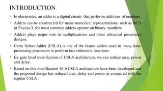
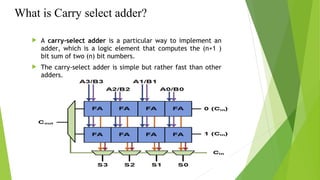
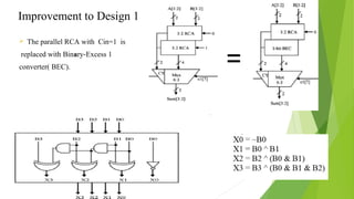
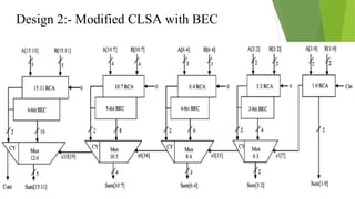
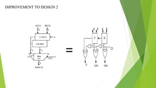
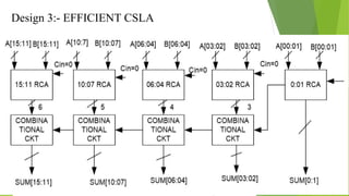
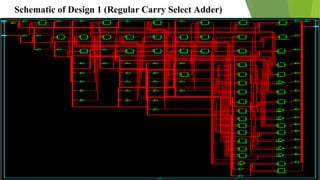
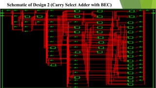
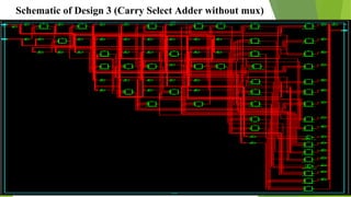
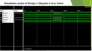
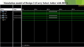
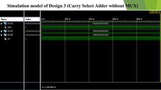
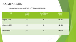
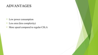
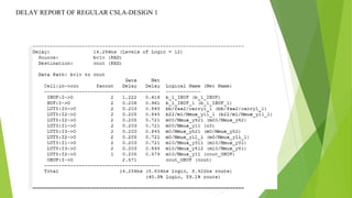
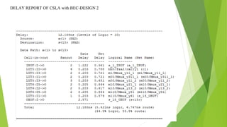
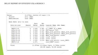
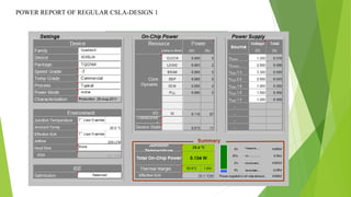
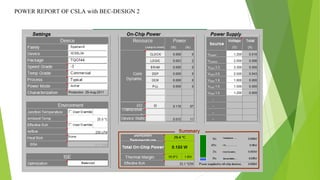
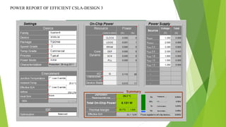
DESIGN AND DEVELOPMENT
OF
EFFICIENT CARRY SELECT ADDER
Presented by:-
ABIN THOMAS, S8, ECE
FEBIN SEBASTIAN, S8, ECE
INTRODUCTION
 In electronics, an adder is a digital circuit that performs addition of numbers.
 Adders can be constructed for many numerical representations, such as BCD
or Excess-3, the most common adders operate on binary numbers.
 Adders plays major role in multiplications and other advanced processors
designs.
 Carry Select Adder (CSLA) is one of the fastest adders used in many data-
processing processors to perform fast arithmetic functions.
 By gate level modification of CSLA architecture, we can reduce area, power
and delay.
 Based on this modification 16-b CSLA architecture have been developed and
the proposed design has reduced area, delay and power as compared with the
regular CSLA .
RIPPLE CARRY ADDER(RCA)
 This kind of adder is a Ripple Carry Adder, since each carry
bit "ripples" to the next full adder.
 The first (and only the first) full adder may be replaced by
a half adder.
What is Carry select adder?
 A carry-select adder is a particular way to implement an
adder, which is a logic element that computes the (n+1 )
bit sum of two (n) bit numbers.
 The carry-select adder is simple but rather fast than other
adders.
Design 1:- Regular 16 bit CSLA
Design 2:- 16 bit CSLA with BEC
Design 3:- 16 bit EFFICIENT CSLA
OUR PROJECT
EXISTING SYSTEM
The carry-select adder generally consists of two Ripple Carry
Adders (RCA) and a Multiplexer .
Adding two n-bit numbers with a carry-select adder is done with
two adders (therefore two RCA).
In order to perform the calculation twice, one time with the assumption
of the carry being zero and the other assuming one.
Design 1:- REGULAR 16bit CSLA
Model of Carry Select Adder
Improvement to Design 1
 The parallel RCA with Cin=1 is
replaced with Binary-Excess 1
converter( BEC). =
Design 2:- Modified CLSA with BEC
=
IMPROVEMENT TO DESIGN 2
Design 3:- EFFICIENT CSLA
Tools used:
 Iverilog 0.10.0
 Isim
 Xilinx ISE 14.7
 Xilinx Spreadsheet
Schematic and Simulation Results:-
Schematic of Design 1 (Regular Carry Select Adder)
Schematic of Design 2 (Carry Select Adder with BEC)
Schematic of Design 3 (Carry Select Adder without mux)
Simulation model of Design 1 (Regular Carry Select
Adder)
Simulation model of Design 2 (Carry Select Adder with BEC)
Simulation model of Design 3 (Carry Select Adder without MUX)
COMPARISON
TYPE POWER
(mW)
No. of Slices
(= area)
DELAY
(ns)
Regular CSLA 134 46 14.256
CSLA with BEC 133 31 12.188
Efficient CSLA 131 11 11.974
 Comparison done in SPARTAN 6 FPGA xc6slx4-3tqg144
ADVANTAGES
 Low power consumption
 Less area (less complexity)
 More speed compared to regular CSLA
CONCLUSION
A simple approach is proposed in this project to reduce the area
and power of CSLA architecture. The reduced number of gates of
this work offers the great advantage in the reduction of area and
also the power. The modified CSLA architecture is therefore, low
area, low power, simple and efficient for VLSI hardware
implementation.
REFERENCE
[1] Laxman Shanigarapu, Bhavana P. Shrivastava ”Area and power efficient carry select
adder” IJIRTS,Vol.1,2013
[2] B. Ramkumar, Harish M Kittur “Low power and Area efficient carry select
adder,”IEEE Trans,Vol.20,Feb 2012.
[3] Y. Kim and L.-S. Kim, “64-bit carry-select adder with reduced area,” Electron. Lett.,
vol. 37, no. 10, pp. 614–615, May 2001.
[4] T. Y. Ceiang and M. J. Hsiao, “Carry-select adder using single ripple carry adder,”
Electron. Lett., vol. 34, no. 22, pp. 2101–2103, Oct. 1998.
[5] Samir Palnitkar, “Verilog Hdl: A Guide to Digital Design and Synthesis”2005,2nd
Edition.
[6] J. M. Rabaey, Digtal Integrated Circuits—A Design Perspective.Upper Saddle River,
NJ: Prentice-Hall, 2001.
DELAY REPORT OF REGULAR CSLA-DESIGN 1
DELAY REPORT OF CSLA with BEC-DESIGN 2
DELAY REPORT OF EFFICIENT CSLA-DESIGN 3
POWER REPORT OF REGULAR CSLA-DESIGN 1
POWER REPORT OF CSLA with BEC-DESIGN 2
POWER REPORT OF EFFICIENT CSLA-DESIGN 3

Design and development of carry select adder

  • 1.
    DESIGN AND DEVELOPMENT OF EFFICIENTCARRY SELECT ADDER Presented by:- ABIN THOMAS, S8, ECE FEBIN SEBASTIAN, S8, ECE
  • 2.
    INTRODUCTION  In electronics,an adder is a digital circuit that performs addition of numbers.  Adders can be constructed for many numerical representations, such as BCD or Excess-3, the most common adders operate on binary numbers.  Adders plays major role in multiplications and other advanced processors designs.  Carry Select Adder (CSLA) is one of the fastest adders used in many data- processing processors to perform fast arithmetic functions.  By gate level modification of CSLA architecture, we can reduce area, power and delay.  Based on this modification 16-b CSLA architecture have been developed and the proposed design has reduced area, delay and power as compared with the regular CSLA .
  • 3.
    RIPPLE CARRY ADDER(RCA) This kind of adder is a Ripple Carry Adder, since each carry bit "ripples" to the next full adder.  The first (and only the first) full adder may be replaced by a half adder.
  • 4.
    What is Carryselect adder?  A carry-select adder is a particular way to implement an adder, which is a logic element that computes the (n+1 ) bit sum of two (n) bit numbers.  The carry-select adder is simple but rather fast than other adders.
  • 5.
    Design 1:- Regular16 bit CSLA Design 2:- 16 bit CSLA with BEC Design 3:- 16 bit EFFICIENT CSLA OUR PROJECT
  • 6.
    EXISTING SYSTEM The carry-selectadder generally consists of two Ripple Carry Adders (RCA) and a Multiplexer . Adding two n-bit numbers with a carry-select adder is done with two adders (therefore two RCA). In order to perform the calculation twice, one time with the assumption of the carry being zero and the other assuming one.
  • 7.
  • 8.
    Model of CarrySelect Adder
  • 9.
    Improvement to Design1  The parallel RCA with Cin=1 is replaced with Binary-Excess 1 converter( BEC). =
  • 10.
    Design 2:- ModifiedCLSA with BEC
  • 11.
  • 12.
  • 13.
    Tools used:  Iverilog0.10.0  Isim  Xilinx ISE 14.7  Xilinx Spreadsheet
  • 14.
  • 15.
    Schematic of Design1 (Regular Carry Select Adder)
  • 16.
    Schematic of Design2 (Carry Select Adder with BEC)
  • 17.
    Schematic of Design3 (Carry Select Adder without mux)
  • 18.
    Simulation model ofDesign 1 (Regular Carry Select Adder)
  • 19.
    Simulation model ofDesign 2 (Carry Select Adder with BEC)
  • 20.
    Simulation model ofDesign 3 (Carry Select Adder without MUX)
  • 21.
    COMPARISON TYPE POWER (mW) No. ofSlices (= area) DELAY (ns) Regular CSLA 134 46 14.256 CSLA with BEC 133 31 12.188 Efficient CSLA 131 11 11.974  Comparison done in SPARTAN 6 FPGA xc6slx4-3tqg144
  • 22.
    ADVANTAGES  Low powerconsumption  Less area (less complexity)  More speed compared to regular CSLA
  • 23.
    CONCLUSION A simple approachis proposed in this project to reduce the area and power of CSLA architecture. The reduced number of gates of this work offers the great advantage in the reduction of area and also the power. The modified CSLA architecture is therefore, low area, low power, simple and efficient for VLSI hardware implementation.
  • 24.
    REFERENCE [1] Laxman Shanigarapu,Bhavana P. Shrivastava ”Area and power efficient carry select adder” IJIRTS,Vol.1,2013 [2] B. Ramkumar, Harish M Kittur “Low power and Area efficient carry select adder,”IEEE Trans,Vol.20,Feb 2012. [3] Y. Kim and L.-S. Kim, “64-bit carry-select adder with reduced area,” Electron. Lett., vol. 37, no. 10, pp. 614–615, May 2001. [4] T. Y. Ceiang and M. J. Hsiao, “Carry-select adder using single ripple carry adder,” Electron. Lett., vol. 34, no. 22, pp. 2101–2103, Oct. 1998. [5] Samir Palnitkar, “Verilog Hdl: A Guide to Digital Design and Synthesis”2005,2nd Edition. [6] J. M. Rabaey, Digtal Integrated Circuits—A Design Perspective.Upper Saddle River, NJ: Prentice-Hall, 2001.
  • 26.
    DELAY REPORT OFREGULAR CSLA-DESIGN 1
  • 27.
    DELAY REPORT OFCSLA with BEC-DESIGN 2
  • 28.
    DELAY REPORT OFEFFICIENT CSLA-DESIGN 3
  • 29.
    POWER REPORT OFREGULAR CSLA-DESIGN 1
  • 30.
    POWER REPORT OFCSLA with BEC-DESIGN 2
  • 31.
    POWER REPORT OFEFFICIENT CSLA-DESIGN 3