Vikas Kumar has experience in designing and implementing various digital and analog circuits including a 32-bit RISC CPU using Verilog, an integrated round robin arbiter on an FPGA board, asynchronous and synchronous FIFOs for clock domain crossing, a two-stage op-amp using UMC 180nm technology, and a bandgap reference circuit. He has worked as an intern at KeenHeads Technologies and IISc Bangalore developing projects related to analog design, layout design, and an embedded security system. Vikas has skills in RTL coding, digital and analog design, layout design, Verilog, C/C++, MATLAB, and uses tools including Xilinx Vivado, Cad
FPGA are a special form of Programmable logic devices(PLDs) with higher densities as compared to custom ICs and capable of implementing functionality in a short period of time using computer aided design (CAD) software....by mathewsubin3388@gmail.com
I made this presentation for you , I hope its useful for you all, and I hate Plagiarism please, I also used some slides here but I mentioned all in the last slide :)
Hope you can get benefits from it
In this presentation of mine, a basic Design approach of VLSI has been explained. The ppt explains the market level of VLSI and also the fabrication process and also its various applications. An integration of various switches, gates, etc on Ic's has also been showcased in the same.
Problems of dynamic logic circuits and how it is solved by Domino logic circuits, is explained over here. Why it is called domino and how domino logic works, that also explained here.
Complex Programmable Logic Device (CPLD) Architecture and Its Applicationselprocus
A CPLD (complex programmable logic device) chip includes several circuit blocks on a single chip with inside wiring resources to attach the circuit blocks. Each circuit block is comparable to a PLA or a PAL.
VLSI stands for Very Large Scale integration is the art of integrating millions of transistors on a Silicon Chip. Researchers are working to incorporate large scale integration of electronic devices on a single silica chip “Integrated Circuit or IC” to fulfill the market demand. Here, in this presentation we will learn introduction and history of VLSI, VLSI Design Style and Flow, VLSI Design Approaches, CPLD, FPGA, Programmable Logic Arrays, Xilinx vs. Altera Design tools, flow and files.
Those slides describe digital design using Verilog HDL,
starting with Design methodologies for any digital circuit then difference between s/w (C/C++) and H/w (Verilog) and the most important constructs that let us start hardware design using Verilog HDL.
DESIGN AND SIMULATION OF DIFFERENT 8-BIT MULTIPLIERS USING VERILOG CODE BY SA...Saikiran Panjala
In this project, we compare the working of the four 8- bit multipliers like Wallace tree multiplier, Array multiplier, Baugh-Wooley multiplier and Vedic multiplier by simulating each of them separately. This is a very important criterion because in the fabrication of chips and the high-performance system requires components which are as small as possible.
If you any doubts regarding project.......then to a mail(saikiranpanjala@gmail.com)
The journey of designing an ASIC (application specific integrated circuit) is long and involves a number of major steps – moving from a concept to specification to tape-outs. Although the end product is typically quite small (measured in nanometers), this long journey is interesting and filled with many engineering challenges.
Today, ASIC design flow is a very mature process in silicon turnkey design. The ASIC design flow and its various steps in VLSI engineering that we describe below are based on best practices and proven methodologies in ASIC chip designs. This blog attempts to explain different steps in the ASIC design flow, starting from ASIC design concept and moving from specifications to benefits.
To ensure successful ASIC design, engineers must follow a proven ASIC design flow which is based on a good understanding of ASIC specifications, requirements, low power design and performance, with a focus on meeting the goal of right time to market. Every stage of ASIC design cycle has EDA tools that can help to implement ASIC design with ease.
6 months/weeks training in Vlsi,jalandhardeepikakaler1
E2marix is leading Training & Certification Company offering Corporate Training Programs, IT Education Courses in diversified areas.Since its inception, E2matrix educational Services have trained and certified many students and professionals.
TECHNOLOGIES PROVIDED -
MATLAB
NS2
IMAGE PROCESSING
.NET
SOFTWARE TESTING
DATA MINING
NEURAL networks
HFSS
WEKA
ANDROID
CLOUD computing
COMPUTER NETWORKS
FUZZY LOGIC
ARTIFICIAL INTELLIGENCE
LABVIEW
EMBEDDED
VLSI
Address
Opp. Phagwara Bus Stand, Above Bella
Pizza, Handa City Center, Phagwara
email-e2matrixphagwara@gmail.com
jalandhare2matrix@gmail.com
Web site-www.e2matrix.com
CONTACT NUMBER --
07508509730
09041262727
7508509709
6 weeks/months summer training in vlsi,ludhianadeepikakaler1
E2matrix offer our assistance, writing and consulting services with your research assignments particularly in the areas of thesis, dissertations, journals, online forum discussions, FYP, and so on.
We also provide training for the different technologies and are involved in a wide diversity of subject areas ranging from management,engineering up to programming and designs; and our team of research experts and professional consultants are readily available to help you towards your successful completion of your assignments.
Engage us today at our e2matrixphagwara@gmail.com
jalandhare2matrix@gmail.com
and can visit our web site-www.e2matrix.com
contact us-7508509709
07508509730
Presentation made by Jose Pinilla and Alfredo Gualdrón to show the CSTAR (Canadian Surgical Technologies and Advanced Robotics) how FPGAs are being used in the Universidad Pontificia Bolivariana in Bucaramanga, Colombia.
Product Engineering Company- IoT, Semiconductor & Systems. MosChip is Product Development company with over 16+ years of extensive expertise in semiconductor / systems / IoT engineering from SoC (Systems on Chip), Embedded Systems Design, Cloud and Mobile Software development catering to the Aerospace & Defence, Consumer Electronics, Automotive, Medical, Telecommunications, Mobile industries.
With over 400+ Clients in 140 countries, Moschip has also put its footprint in the field of IoT, Cloud and Connected Devices domain. Driven by a positive outlook, Moschip is moving to more flexible, agile models.
https://moschip.com
E2MATRIX PROVIDE EXPERT GUIDANCE FOR THESIS & PROJECT FOR M.TECH. / PHD / B.TECH. STUDENTS. MTECH THESIS/ IEEE PROJECT GUIDANCE / PHD THESIS. GENUINE THESIS / PROJECT WORK BY THE EXPERT FACULTY/ DEVELOPERS. DOMAINS / TECHNOLOGIES - MATLAB NS2 IMAGE PROCESSING .NET WIRELESS COMMUNICATION DATA MINING NEURAL NETWORKS HFSS / IE3D ANTENNA WEKA ANDROID CLOUD COMPUTING FUZZY LOGIC ARTIFICIAL INTELLIGENCE LABVIEW EMBEDDED VLSI AND MANY MORE. WE PROVIDE- RESEARCH PAPERS OBJECTIVES SYNOPSIS IMPLEMENTATION DOCUMENTATION REPORT WRITING PAPER PUBLICATION FOR MORE INFORMATION
contact us -
Address-Opp. Phagwara Bus Stand, Above Bella
Pizza, Handa City Center, Phagwara,punjab
email addres-e2matrixphagwara@gmail.com
jalandhare2matrix@gmail.com
WEBSITE-www.e2matrix.com
CONTACT NUMBER --
09041262727
07508509730
7508509709
COLLEGE BUS MANAGEMENT SYSTEM PROJECT REPORT.pdfKamal Acharya
The College Bus Management system is completely developed by Visual Basic .NET Version. The application is connect with most secured database language MS SQL Server. The application is develop by using best combination of front-end and back-end languages. The application is totally design like flat user interface. This flat user interface is more attractive user interface in 2017. The application is gives more important to the system functionality. The application is to manage the student’s details, driver’s details, bus details, bus route details, bus fees details and more. The application has only one unit for admin. The admin can manage the entire application. The admin can login into the application by using username and password of the admin. The application is develop for big and small colleges. It is more user friendly for non-computer person. Even they can easily learn how to manage the application within hours. The application is more secure by the admin. The system will give an effective output for the VB.Net and SQL Server given as input to the system. The compiled java program given as input to the system, after scanning the program will generate different reports. The application generates the report for users. The admin can view and download the report of the data. The application deliver the excel format reports. Because, excel formatted reports is very easy to understand the income and expense of the college bus. This application is mainly develop for windows operating system users. In 2017, 73% of people enterprises are using windows operating system. So the application will easily install for all the windows operating system users. The application-developed size is very low. The application consumes very low space in disk. Therefore, the user can allocate very minimum local disk space for this application.
Industrial Training at Shahjalal Fertilizer Company Limited (SFCL)MdTanvirMahtab2
This presentation is about the working procedure of Shahjalal Fertilizer Company Limited (SFCL). A Govt. owned Company of Bangladesh Chemical Industries Corporation under Ministry of Industries.
Vaccine management system project report documentation..pdfKamal Acharya
The Division of Vaccine and Immunization is facing increasing difficulty monitoring vaccines and other commodities distribution once they have been distributed from the national stores. With the introduction of new vaccines, more challenges have been anticipated with this additions posing serious threat to the already over strained vaccine supply chain system in Kenya.
Cosmetic shop management system project report.pdfKamal Acharya
Buying new cosmetic products is difficult. It can even be scary for those who have sensitive skin and are prone to skin trouble. The information needed to alleviate this problem is on the back of each product, but it's thought to interpret those ingredient lists unless you have a background in chemistry.
Instead of buying and hoping for the best, we can use data science to help us predict which products may be good fits for us. It includes various function programs to do the above mentioned tasks.
Data file handling has been effectively used in the program.
The automated cosmetic shop management system should deal with the automation of general workflow and administration process of the shop. The main processes of the system focus on customer's request where the system is able to search the most appropriate products and deliver it to the customers. It should help the employees to quickly identify the list of cosmetic product that have reached the minimum quantity and also keep a track of expired date for each cosmetic product. It should help the employees to find the rack number in which the product is placed.It is also Faster and more efficient way.
Forklift Classes Overview by Intella PartsIntella Parts
Discover the different forklift classes and their specific applications. Learn how to choose the right forklift for your needs to ensure safety, efficiency, and compliance in your operations.
For more technical information, visit our website https://intellaparts.com
Welcome to WIPAC Monthly the magazine brought to you by the LinkedIn Group Water Industry Process Automation & Control.
In this month's edition, along with this month's industry news to celebrate the 13 years since the group was created we have articles including
A case study of the used of Advanced Process Control at the Wastewater Treatment works at Lleida in Spain
A look back on an article on smart wastewater networks in order to see how the industry has measured up in the interim around the adoption of Digital Transformation in the Water Industry.
Immunizing Image Classifiers Against Localized Adversary Attacksgerogepatton
This paper addresses the vulnerability of deep learning models, particularly convolutional neural networks
(CNN)s, to adversarial attacks and presents a proactive training technique designed to counter them. We
introduce a novel volumization algorithm, which transforms 2D images into 3D volumetric representations.
When combined with 3D convolution and deep curriculum learning optimization (CLO), itsignificantly improves
the immunity of models against localized universal attacks by up to 40%. We evaluate our proposed approach
using contemporary CNN architectures and the modified Canadian Institute for Advanced Research (CIFAR-10
and CIFAR-100) and ImageNet Large Scale Visual Recognition Challenge (ILSVRC12) datasets, showcasing
accuracy improvements over previous techniques. The results indicate that the combination of the volumetric
input and curriculum learning holds significant promise for mitigating adversarial attacks without necessitating
adversary training.
Explore the innovative world of trenchless pipe repair with our comprehensive guide, "The Benefits and Techniques of Trenchless Pipe Repair." This document delves into the modern methods of repairing underground pipes without the need for extensive excavation, highlighting the numerous advantages and the latest techniques used in the industry.
Learn about the cost savings, reduced environmental impact, and minimal disruption associated with trenchless technology. Discover detailed explanations of popular techniques such as pipe bursting, cured-in-place pipe (CIPP) lining, and directional drilling. Understand how these methods can be applied to various types of infrastructure, from residential plumbing to large-scale municipal systems.
Ideal for homeowners, contractors, engineers, and anyone interested in modern plumbing solutions, this guide provides valuable insights into why trenchless pipe repair is becoming the preferred choice for pipe rehabilitation. Stay informed about the latest advancements and best practices in the field.
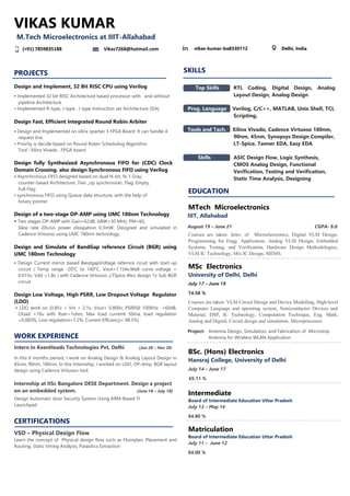
1. VIKAS KUMAR
M.Tech Microelectronics at IIIT-Allahabad
(+91) 7859835188 Vikas7268@hotmail.com
PROJECTS
Design and Implement, 32 Bit RISC CPU using Verilog
• Implemented 32 bit RISC Architecture based processor with and without
pipeline Architecture
• Implemented R-type, J-type , I-type Instruction set Architecture (ISA)
Design Fast, Efficient Integrated Round Robin Arbiter
• Design and Implemented on xilinx spartan 3 FPGA Board. It can handle 4
request line.
• Priority is decide based on Round Robin Scheduling Algorithm.
Tool : Xilinx Vivado , FPGA board
Design fully Synthesized Asynchronous FIFO for (CDC) Clock
Domain Crossing. also design Synchronous FIFO using Verilog
• Asynchronous FIFO designed based on dual N-bit, N-1 Gray
counter-based Architecture, Two _op synchronizer, Flag: Empty,
Full Flag
• synchronous FIFO using Queue data structure, with the help of
binary pointer.
Design of a two-stage OP-AMP using UMC 180nm Technology
• Two stages OP-AMP with Gain=62dB, GBW=30 MHz, PM=60,
Slew rate 20v/us power dissipation 0.3mW. Designed and simulated in
Cadence Virtuoso using UMC 180nm technology.
Design and Simulate of BandGap reference Circuit (BGR) using
UMC 180nm Technology
• Design Current mirror based BandgapVoltage refernce cicuit with start-up
circuit ( Temp range -20°C to 140°C, Vout=1.154v,Well curve voltage =
0.015v, Vdd =1.8v ) with Cadence Virtuoso ,LTSpice Also design 1v Sub BGR
circuit
Design Low Voltage, High PSRR, Low Dropout Voltage Regulator
(LDO)
• LDO work on (0.85v < Vin < 2.1v, Vout= 0.800v, PSRR@ 100KHz =60dB,
Cload =10u with Rser=1ohm, Max load curremt 50ma, load regulation
=0.083%, Line regulation=1.2%, Current Efficency= 98.5%)
WORK EXPERIENCE
Intern in KeenHeads Technologies Pvt, Delhi (Jun 20 – Nov 20)
In this 6 months period, I work on Analog Design & Analog Layout Design in
45nm, 90nm, 180nm. In this Internship, I worked on LDO, OP-Amp, BGR layout
design using Cadence Virtuoso tool.
Internship at IISc Bangalore DESE Department. Design a project
on an embedded system. (June 18 – July 18)
Design Automatic door Security System Using ARM-Based TI
Launchpad
CERTIFICATIONS
VSD – Physical Design Flow
Learn the concept of Physical design flow such as Floorplan, Placement and
Routing, Static timing Analysis, Parasitics Extraction
vikas-kumar-ba8330112 Delhi, India
SKILLS
Top Skills RTL Coding, Digital Design, Analog
Layout Design, Analog Design
Prog. Language Verilog, C/C++, MATLAB, Unix Shell, TCL
Scripting,
Tools and Tach. Xilinx Vivado, Cadence Virtuoso 180nm,
90nm, 45nm, Synopsys Design Compiler,
LT-Spice, Tanner EDA, Easy EDA
Skills ASIC Design Flow, Logic Synthesis,
CMOS Analog Design, Functional
Verification, Testing and Verification,
Static Time Analysis, Designing
EDUCATION
MTech Microelectronics
IIIT, Allahabad
August 19 – June 21 CGPA- 8.0
Courses are taken: Intro. of Microelectronics, Digital VLSI Design,
Programming for Engg. Application, Analog VLSI Design, Embedded
Systems, Testing, and Verification, Hardware Design Methodologies,
VLSI IC Technology, Mix IC Design, MEMS.
MSc Electronics
University of Delhi, Delhi
July 17 – June 19
74.50 %
Courses are taken: VLSI Circuit Design and Device Modelling, High-level
Computer Language and operating system, Semiconductor Devices and
Material, DSP, IC Technology, Computation Technique, Eng. Math,
Analog and Digital, Circuit design and simulation, Microprocessor.
Project- Antenna Design, Simulation, and Fabrication of Microstrip
Antenna for Wireless WLAN Application
BSc. (Hons) Electronics
Hansraj College, University of Delhi
July 14 – June 17
65.11 %
Intermediate
Board of Intermediate Education Uttar Pradesh
July 13 – May 14
84.80 %
Matriculation
Board of Intermediate Education Uttar Pradesh
July 11 – June 12
84.00 %