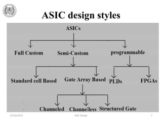
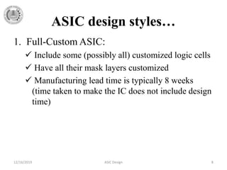
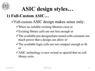
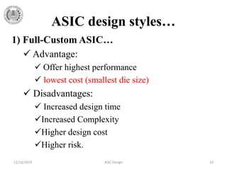
An application-specific IC (ASIC) can be either a digital or an analog circuit. As their name implies, ASICs are not reconfigurable; they perform only one specific function. For example, a speed controller IC for a remote control car is hard-wired to do one job and could never become a microprocessor. An ASIC does not contain any ability to follow alternate instructions.
The document describes the ASIC design flow, which consists of two main phases: logical design (frontend) and physical design (backend).
The logical design phase includes design entry, logic synthesis, system partitioning, and pre-layout simulation. This phase converts the design from HDL or schematic to a netlist.
The physical design phase includes floorplanning, placement, routing, circuit extraction, and post-layout simulation. This phase adds physical details and checks timing with parasitics. Floorplanning places blocks, placement assigns cell locations, and routing connects cells and blocks. Circuit extraction determines resistances and capacitances, and post-layout simulation verifies functionality and timing.
The VLSI design flow consists of three domains - behavioral, structural, and physical - and multiple levels from system to circuit level. The front-end design includes logic synthesis to generate a netlist from HDL code through technology mapping and optimization. Back-end physical design involves floorplanning, placement of cells, routing of interconnects, and simulation to verify functionality and timing.
Low power VLSI design has become an important discipline due to increasing device densities, operating frequencies, and proliferation of portable electronics. Power dissipation, which was previously neglected, is now a primary design constraint. There are several sources of power dissipation in CMOS circuits, including switching power due to charging and discharging capacitances, short-circuit power during signal transitions, and leakage power from subthreshold and gate leakage currents. Designers have some control over power consumption by optimizing factors such as activity levels, clock frequency, supply voltage, transistor sizing and architecture.
An FPGA is a programmable logic device containing an array of configurable logic blocks and interconnects that can be programmed to perform different logic functions. It allows reprogramming to perform different functions in microseconds. The key parts of an FPGA are I/O blocks around the edge to interface with other components, logic blocks in the interior to implement logic functions, and interconnects to connect the blocks. FPGAs are programmed by configuring electronic switches to define logic functions and connect the blocks as required.
This document discusses multi mode multi corner (MMMC) analysis for chip design. It defines that a mode is a set of design parameters like clocks and timing constraints, and a corner captures process, voltage, and temperature variations. It provides examples of multiple modes like normal, sleep, and test modes and corners for temperature, voltage, process variations, and parasitic interconnects. The document gives an example of analyzing a chip with 4 modes under 3 process-voltage-temperature corners and 3 parasitic interconnect corners, showing 9 analysis cases.
This document outlines the typical design flow for VLSI chips, including: 1) design specification, 2) design entry using schematics or HDL, 3) functional simulation to verify logic, 4) planning placement and routing of components, 5) timing simulation accounting for delays, and 6) fabrication of the final chip design either using full custom or semi-custom methods. The goal is to design and test a chip that meets the specified requirements before manufacturing.
The document discusses placement in physical design. It describes placement as assigning positions to predesigned cells on a chip without overlapping to optimize objectives like minimizing area and interconnects. It discusses different placement types, formulates the placement problem, and describes algorithms like partitioning-based placement, simulated annealing placement, and iterative placement methods.
This document outlines the syllabus for a VLSI design course. The syllabus covers five units: (1) CMOS technology, including history, characteristics, and enhancements; (2) circuit characterization and simulation; (3) combinational and sequential circuit design; (4) CMOS testing; and (5) specification using Verilog HDL. The first unit provides an introduction to CMOS technology, discussing MOS transistors, CMOS processes like p-well and n-well, and layout design rules. Subsequent units cover circuit analysis, common circuit elements, testing approaches, and hardware description languages. References include textbooks on VLSI design, digital circuits, and Verilog HDL.
This document provides an introduction to electronic design automation (EDA) tools and discusses different types of programmable logic devices including field programmable gate arrays (FPGAs) and complex programmable logic devices (CPLDs). It describes the basic architecture of FPGAs including logic blocks, interconnects, and input/output blocks. The advantages of FPGAs such as shorter development time and flexibility are also summarized.
This document provides an overview of application specific integrated circuits (ASICs). It discusses the main types of ASICs including full custom, semi-custom (standard cell-based and gate array-based), and programmable. For semi-custom, it describes standard cell-based ASICs using predesigned logic cells and different types of gate arrays including channeled, channelless, and structured. The document also covers the design flow, economics, merits like improved speed and power consumption, and demirts such as high costs for redesigns.
The document discusses a 5T SRAM cell for embedded cache memory. It begins by explaining the basic operations of memory and different types of memory like RAM and ROM. It then discusses the structure and operation of a typical 6T SRAM cell. It introduces a 5T SRAM cell that aims to reduce leakage and increase density compared to 6T cells. The document outlines the read and write operations of the 5T cell and provides results of implementing the cell showing improvements in leakage and area. It concludes by discussing potential applications and areas for future work.
This document discusses the programming technologies and interconnect architectures used in different FPGA devices. It covers antifuse-based OTP technologies used in Actel FPGAs, SRAM-based reprogrammable technologies used in Xilinx FPGAs, and EPROM/EEPROM technologies used in Altera CPLDs. It also describes the segmented channel routing interconnect architecture used in Actel FPGAs and the LCA architecture used in Xilinx FPGAs.
The physical design flow begins with placement which involves assigning exact locations to modules like gates and standard cells to minimize area and interconnect cost while meeting timing constraints, with the goal of enabling easier routing; placement tools take as input the netlist, floorplan, libraries, and constraints to perform global and detailed placement as well as optimization. The quality of placement significantly impacts the ability to route the design successfully.
This document provides an overview of the syllabus for a course on VLSI Design. It discusses the teaching scheme, examination scheme, and various units that will be covered in the course, including VHDL modeling, finite state machines, programmable logic devices, system on chip design, CMOS VLSI design, and testability. It also lists recommended textbooks and reference books and provides a list of potential experiments for the practical component of the course.
Routing in Integrated circuits is an important task which requires extreme care while placing the modules and circuits and connecting them with each other.
Intellectual property (IP) in VLSI design refers to reusable logic or functionality units that can be licensed and used as building blocks in chip designs. There are two main types of IP: hard IP, which includes a pre-designed layout, and soft IP, which is delivered as synthesizable code. Soft IP is more vulnerable to theft since it is in a synthesizable form. Memories are often delivered as hard IP since they require careful analog design and peripheral circuitry to be useful. IP differs from custom chip design in that it is created before a specific use, with the goal of reuse across multiple designs. The IP lifecycle involves initial creation through specification, design, testing, and documentation, followed by integration into
Application specific integrated circuits (ASICs) are microchips designed for special applications. There are two types: full-custom ASICs where all logic cells and mask layers are customized, and semi-custom where pre-designed logic cells have some customizable mask layers. ASICs have advantages over FPGAs like lower costs, higher speeds, and lower power usage, but have higher design costs and longer development times. Common applications of ASICs include aerospace systems, high-performance processors, and specialized consumer electronics.
This document outlines the typical ASIC design flow process. It begins with specification where the features and functionalities of the ASIC are defined. This is followed by RTL coding to develop the logic functionality in a hardware description language. Simulation and synthesis then convert the RTL into a gate-level netlist. Pre-layout timing analysis checks for timing issues. Then automatic place and route lays out the design on the chip. Back annotation adds layout parasitic information. Post-layout timing analysis checks for real timing violations. Logic verification confirms correct functionality. The final tapeout step sends the design for fabrication if all checks pass.
This document discusses packaging considerations for VLSI devices. It covers package types like through-hole packages, surface-mounted packages, flip chip packages, and chip-scale packages. Key package design considerations include the number of terminals, electrical design to minimize signal degradation, thermal design to dissipate heat, reliability over temperature cycles, and testability to ensure quality. The ideal package is compact with low-inductance connections to transfer heat efficiently while withstanding stresses.
This document summarizes a research paper that proposes a low power 11T SRAM cell using a Schmitt trigger. It begins by introducing the need for low power VLSI circuits and operation in the sub-threshold region. It then describes existing 6T and 7T SRAM cell designs and discusses schmitt triggers. The proposed 11T SRAM cell replaces the cross-coupled inverters in previous designs with a schmitt trigger pair. Simulation results show the proposed cell reduces power consumption and delay compared to existing cells. In conclusion, the proposed 11T SRAM cell is better suited for low power applications due to its lower power-delay product.
This document discusses various low power techniques for integrated circuits. It begins by describing the increasing challenges of power consumption as device densities and clock frequencies increase while supply voltages and threshold voltages decrease. It then discusses different types of power consumption, including dynamic power, static power, leakage power from different sources, and how they can be reduced. The document covers many low power design techniques like multi-threshold CMOS, clock gating, multi-voltage, DVFS, and more. It discusses the evolution of these techniques and challenges in their implementation like timing issues, level shifters, and floorplanning for multi-voltage designs.
This document provides an overview of VLSI technology trends over time. It discusses how Moore's Law has been sustained through transistor scaling down to the nanometer level enabled by various techniques like strained silicon, high-k dielectrics, metal gates, SOI, multi-gate transistors like FinFETs. It outlines the evolution from bipolar junction transistors to MOSFETs to integrated circuits. Short channel effects posed challenges to scaling which were addressed through new device architectures in the second generation of scaling.
A VLSI (Very Large Scale Integration) system integrates millions of “electronic components” in a small area (few mm2 few cm2).
design “efficient” VLSI systems that has:
Circuit Speed ( high )
Power consumption ( low )
Design Area ( low )
System partitioning in VLSI and its considerationsSubash John
System partitioning divides a large circuit into smaller subcircuits. This allows the subcircuits to be designed independently and in parallel, speeding up the design process. Effective partitioning aims to minimize connections between subcircuits. Tool-based partitioning allows constraints to be set to generate a partitioned netlist that balances subcircuit sizes and minimizes connections between top-level blocks.
This document provides information about reversible logic gates and their application in field programmable gate arrays (FPGAs). It describes the design of reversible 4-to-1 multiplexers, D latches, and master-slave flip flops using novel reversible gates. The proposed reversible designs have fewer components and lower cost compared to existing irreversible circuit designs. In conclusion, the document presents the first proposed design of a reversible logic block for FPGAs, improving the efficiency of sequential circuits used to realize FPGA functions.
The document discusses different types of application specific integrated circuits (ASICs). It describes ASICs as integrated circuits customized for a particular application, as opposed to standard integrated circuits. The document outlines two main types of ASICs: full-custom ASICs which have all logic cells and mask layers customized, and semi-custom ASICs which use pre-designed logic cells but have customized mask layers. Within semi-custom ASICs it distinguishes between standard cell-based and gate array-based designs. The document also covers programmable ASICs including PLDs, CPLDs and FPGAs.
The document discusses different types of application specific integrated circuits (ASICs). It describes ASICs as integrated circuits customized for a particular application, such as chips for toys or automotive controls, as opposed to standard integrated circuits. The document summarizes that there are two main types of ASICs: full-custom ASICs that have all logic cells and mask layers customized, and semi-custom ASICs that use pre-designed logic cells with some customized mask layers. Within semi-custom ASICs, the document outlines different design approaches such as standard cell-based and gate array-based designs, as well as programmable ASICs like PLDs, CPLDs, and FPGAs
This document discusses IC design methodology. It explains that there are standard ICs available off-the-shelf as well as application-specific ICs (ASICs) designed for specific purposes. There are three main design methodologies: full custom where all components are custom designed, semi-custom using pre-designed blocks, and programmable logic devices that can be programmed by users. Semi-custom design includes gate arrays using pre-fabricated transistor cells and standard cells from a library that are interconnected. Programmable logic devices allow flexible design and include PLDs, PROMs, PALs, PLAs and FPGAs. Memory in PLDs can be stored using FAMOS transistors, f
The document provides information about ASIC design companies in India and ASIC design. It lists several major Indian companies involved in ASIC design, VLSI design, and electronic design automation tools. It then discusses topics related to ASIC design such as the physical design flow, CAD tools used, types of ASICs including full-custom and semi-custom, and how standard cells are used in semi-custom ASIC design. The document appears to be course material for a class on ASIC design that will cover the overall design flow and hands-on experience with EDA tools.
1) Semi-custom integrated circuits (ASICs) can be categorized as full-custom, cell-based, or gate-array based depending on the level of customization in their design. 2) Cell-based ASICs use pre-designed logic cells (gates, flip-flops) in a customizable layout, balancing performance and design time. 3) Gate-array ASICs have pre-defined transistor patterns and customizable interconnect, allowing faster turnaround than full-custom designs.
FPGAs were introduced in 1984 as a programmable alternative to PLDs. They fill the gap between discrete logic and smaller PLDs on the low end and more expensive ASICs on the high end. The basic elements of an FPGA are configurable logic blocks (CLBs), configurable I/O blocks (IOBs), and a programmable interconnect. FPGAs from vendors like Xilinx and Altera have a regular architecture of CLBs surrounded by IOBs and connected via a hierarchy of programmable interconnects.
This document provides an introduction to semi-custom integrated circuit design and different types of application-specific integrated circuits (ASICs). It discusses the evolution of IC scale and complexity from SSI to VLSI. The main types of ASICs are described as full-custom, cell-based, and gate-array based. Full-custom ASICs have all layers customized, cell-based ASICs use predefined standard cells, and gate-array based ASICs have predefined transistors with customized interconnect. Channeled and channel-less gate arrays are subtypes that differ in routing architecture. The document aims to outline the design approaches and tradeoffs of semi-custom IC design.
The document discusses different types of programmable logic devices including ASIC, FPGA, and CPLD. It describes the design flow for ASICs and lists common EDA tools for synthesis, simulation, and design entry. Key features of FPGAs are explained such as flexibility, density, cost effectiveness, and avoiding problems of ASICs. The internal structures of CPLDs and FPGAs including lookup tables, I/O blocks, and programmable interconnects are covered. Details are provided on Xilinx Spartan-3 series FPGAs and a comparison is made between FPGAs and CPLDs.
Michael John Sebastian Smith - Application-Specific Integrated Circuits-Addis...VisweswaraRaoSamoju
An ASIC (application-specific integrated circuit) is a chip customized for a specific application. There are several types of ASICs including full-custom ASICs where all logic cells and mask layers are customized, and semicustom ASICs where predesigned logic cells are used and some mask layers are customized. Standard-cell based ASICs and gate-array based ASICs are two common types of semicustom ASICs that use predesigned logic cell libraries. Programmable ASICs like FPGAs do not customize any mask layers.
Michael john sebastian smith application-specific integrated circuits-addison...Đình Khanh Nguyễn
1. An ASIC is an application-specific integrated circuit designed for a specific application rather than intended for general use.
2. There are several types of ASICs including full-custom, semicustom, and programmable. Standard-cell based and gate-array based ASICs are two common types of semicustom ASICs that use predesigned logic cells.
3. Full-custom ASICs involve customizing all logic cells and mask layers for a specific application, while semicustom ASICs use predesigned logic cells but customize some mask layers. Programmable ASICs do not customize any mask layers.
The document provides an introduction to application specific integrated circuits (ASICs). It discusses that ASICs are non-standard integrated circuits designed for a specific application. The document then categorizes ASICs into three types: full-custom ASICs which have fully customized logic and mask layers; semi-custom ASICs which use predesigned logic cells and have some customized mask layers; and programmable ASICs. Within semi-custom ASICs, the document describes standard cell based and gate array based ASICs, focusing on the differences between channeled, channelless, and structured gate arrays.
VLSI design involves integrating millions of transistors onto a single chip. There are various design styles including full custom, standard cell, gate array, and FPGA. Full custom designs have fully customized cells and layouts but require more design time. Standard cell and gate array styles use predesigned cells, reducing design time but only customizing interconnect layers. FPGA designs have no custom masks and the fastest design turnaround time.
This document provides an introduction to VLSI design. It begins by defining VLSI as circuits containing over a million switching devices or logic gates. It then discusses the evolution of integrated circuits from SSI to VLSI and the trends in IC technology. The key advantages of MOS technology over BJT are summarized. The document outlines Moore's Law and provides evidence of its accuracy. It introduces the structured design methodology and top-down, bottom-up approaches. The various stages of the VLSI design flow and physical design cycle are described at a high level. Different design styles including full-custom, standard cell-based, and programmable logic are also summarized.
This document discusses three options for implementing digital designs: microcontrollers, ASICs, and FPGAs. It provides details on the differences between FPGAs and microcontrollers, and between FPGAs and ASICs. FPGAs offer reconfigurable hardware, faster speeds than microcontrollers due to parallel processing, and more flexible I/O. However, ASICs are best for high volume manufacturing due to lower costs. The document also provides information on the internal architecture of FPGAs, including configurable logic blocks, look up tables, programmable interconnects, and I/O blocks.
FPGAs are faster, cheaper, and smaller than ASICs for small applications but ASICs are faster, cheaper, and smaller for large, complex applications due to their ability to be optimized for a specific application. FPGAs consume more power and take less time to design than ASICs which require more complex design processes like floor planning and mask production. For these reasons, FPGAs are better for applications requiring fast design time while ASICs are better for high volume applications seeking maximum optimization of speed, cost, size and power.
This document is a resume for Jaydip Patel seeking an internship or entry-level position in VLSI design and validation. It summarizes his education, including an M.S. in Electrical and Electronics Engineering from California State University, Sacramento and a B.S. in Electronics and Communication Engineering from Gujarat University, India. It also lists relevant coursework, professional experience including internships, tools and software skills, and projects in analog and mixed signal design, logic design, computer architecture, and VLSI validation and testing.
FROM FPGA TO ASIC IMPLEMENTATION OF AN OPENRISC BASED SOC FOR VOIP APPLICATIONieijjournal
ASIC (Application Specific Integrated Circuit) design verification takes as long as the designers take to describe, synthesis and implement the design. The hybrid approach, where the design is first prototyped on an FPGA (Field-Programmable Gate Array) platform for functional validation and then implemented as
an ASIC allows earlier defect detection in the design process and thus allows a significant time saving.
This paper deals with a CMOS standard-cell ASIC implementation of a SoC (System on Chip) based on the
OpenRISC processor for Voice over IP (VoIP) application; where a hybrid approach is adopted. The
architecture of the design is mainly based on the reuse of IPs cores described at the RTL level. This RTL code is technology-independent; hence the design can be ported easily from FPGA to ASIC.
FROM FPGA TO ASIC IMPLEMENTATION OF AN OPENRISC BASED SOC FOR VOIP APPLICATIONieijjournal1
ASIC (Application Specific Integrated Circuit) design verification takes as long as the designers take to
describe, synthesis and implement the design. The hybrid approach, where the design is first prototyped on
an FPGA (Field-Programmable Gate Array) platform for functional validation and then implemented as
an ASIC allows earlier defect detection in the design process and thus allows a significant time saving.
This paper deals with a CMOS standard-cell ASIC implementation of a SoC (System on Chip) based on the
OpenRISC processor for Voice over IP (VoIP) application; where a hybrid approach is adopted. The
architecture of the design is mainly based on the reuse of IPs cores described at the RTL level. This RTL
code is technology-independent; hence the design can be ported easily from FPGA to ASIC. Results show
that the SoC occupied the area of 2.64mm². Regarding the power consumption, RTL power estimation is
given.
This educational PPT provides Primary Goals of Network Security, The Security Trinity, Information Security, Risk Assessment, Security Models, Basic Security Terminologies, Threats, Vulnerabilities, and Attacks, Know Yourself - The Threat and Vulnerability Landscape, Privacy, Anonymity and Pseudo-anonymity, Security, Vulnerabilities, Threats and Adversaries, Know Your Enemy - the Current Threat and Vulnerability Landscape, Security Bugs and Vulnerabilities - The Vulnerability Landscape, Malware, viruses, rootkits and RATs
Spyware, Adware, Scareware, PUPs & Browser hijacking, Phishing, Vishing and SMShing, Spamming & Doxing, Security services, Policy, Mechanism, and Standards, and the basic principles and steps of System development. Besides, because of covering the most basic and advanced network and computer security issues, policies, and principles in easy way, it can help you to create an awareness how to use an internet and how to protect your physical as well as logical assets.
This educational power point helps to introduce you about the basic concepts, structures, and functions of Virtual Private Network(VPN) and Internet Protocol security (IPsec).
In this educational power point, networking standard organizations, a brief introduction to local area network technologies, summary of OSI layer modeling and Ethernet standards,... are provided.
This PPT focuses on the basic concepts of routing protocols including the executive summary of basic computer networks.
Regarding to the routing protocol concepts, it gives us a brief information of routing, protocol, routing protocol, types of routing protocol, metrics of a routing protocol algorithms...
The document discusses simulation, modeling, and testing in VLSI design. It covers various topics including logic simulation, fault simulation, and VLSI testing. Logic simulation verifies design correctness using simulation. Fault simulation measures test effectiveness by simulating faults. VLSI testing verifies manufactured chips using test generation and application. The document compares different simulation and testing techniques.
VHDL (VHSIC Hardware Description Language) is becoming increasingly popular as a way to capture complex digital electronic circuits for both simulation and synthesis. Digital circuits captured using VHDL can be easily simulated, are more likely to be synthesizable into multiple target technologies, and can be archived for later modification and reuse.
FPGAs allow for reconfigurable circuitry, easier entry with lower costs, and are well-suited for applications that may require frequent design upgrades. However, FPGAs are less energy efficient, have lower maximum operating frequencies, and do not support analog designs compared to ASICs. While FPGAs are useful for prototyping, ASICs are better suited for high-volume mass production since their circuitry is permanently optimized for a specific application.
This document discusses various local area network (LAN) technologies. It begins by defining LANs and explaining that they can connect devices within a single building or across multiple buildings. Common LAN technologies discussed include Ethernet, Token Ring, fiber, and wireless networks. Ethernet is currently the most widely used standard. Fast Ethernet and Gigabit Ethernet are also covered as higher-speed successors to standard Ethernet. The document also examines protocols, the OSI model, Ethernet coding standards, and different types of media like twisted pair and fiber optic cables.
Basic Computer Organization and Design
.....................................................................
The basic computer design represents all of the major concepts in CPU design without overwhelming students with the complexity of a modern commercial CPU.
Weather forecasting is the application of science and technology to predict the state of the atmosphere for a future time and a given location. Now days, forecasting of accurate atmospheric conditions is the major challenge for the meteorologist and poor forecasting has significant impact on our daily lives. This brings the necessity to make research works on forecasting of the weather events with respect to Ethiopia.
The Globus architecture provides an open source software toolkit that allows sharing of computing power, databases, and other resources across organizational boundaries. It has three main components - resource management, data management, and information services. The core Globus Toolkit components allow users to access remote resources seamlessly while preserving local control. It includes services like the Grid Resource Allocation Manager (GRAM) for job submission and monitoring, the Monitoring and Discovery Service (MDS) for resource information, and Grid FTP for secure data transfer. The Gridbus architecture builds upon Globus to address additional challenges around composing distributed applications, resource brokering, data management, and accounting to support both scientific and business applications on grids.
Gender and Mental Health - Counselling and Family Therapy Applications and In...PsychoTech Services
A proprietary approach developed by bringing together the best of learning theories from Psychology, design principles from the world of visualization, and pedagogical methods from over a decade of training experience, that enables you to: Learn better, faster!
ISO/IEC 27001, ISO/IEC 42001, and GDPR: Best Practices for Implementation and...PECB
Denis is a dynamic and results-driven Chief Information Officer (CIO) with a distinguished career spanning information systems analysis and technical project management. With a proven track record of spearheading the design and delivery of cutting-edge Information Management solutions, he has consistently elevated business operations, streamlined reporting functions, and maximized process efficiency.
Certified as an ISO/IEC 27001: Information Security Management Systems (ISMS) Lead Implementer, Data Protection Officer, and Cyber Risks Analyst, Denis brings a heightened focus on data security, privacy, and cyber resilience to every endeavor.
His expertise extends across a diverse spectrum of reporting, database, and web development applications, underpinned by an exceptional grasp of data storage and virtualization technologies. His proficiency in application testing, database administration, and data cleansing ensures seamless execution of complex projects.
What sets Denis apart is his comprehensive understanding of Business and Systems Analysis technologies, honed through involvement in all phases of the Software Development Lifecycle (SDLC). From meticulous requirements gathering to precise analysis, innovative design, rigorous development, thorough testing, and successful implementation, he has consistently delivered exceptional results.
Throughout his career, he has taken on multifaceted roles, from leading technical project management teams to owning solutions that drive operational excellence. His conscientious and proactive approach is unwavering, whether he is working independently or collaboratively within a team. His ability to connect with colleagues on a personal level underscores his commitment to fostering a harmonious and productive workplace environment.
Date: May 29, 2024
Tags: Information Security, ISO/IEC 27001, ISO/IEC 42001, Artificial Intelligence, GDPR
-------------------------------------------------------------------------------
Find out more about ISO training and certification services
Training: ISO/IEC 27001 Information Security Management System - EN | PECB
ISO/IEC 42001 Artificial Intelligence Management System - EN | PECB
General Data Protection Regulation (GDPR) - Training Courses - EN | PECB
Webinars: https://pecb.com/webinars
Article: https://pecb.com/article
-------------------------------------------------------------------------------
For more information about PECB:
Website: https://pecb.com/
LinkedIn: https://www.linkedin.com/company/pecb/
Facebook: https://www.facebook.com/PECBInternational/
Slideshare: http://www.slideshare.net/PECBCERTIFICATION
How to Make a Field Mandatory in Odoo 17Celine George
In Odoo, making a field required can be done through both Python code and XML views. When you set the required attribute to True in Python code, it makes the field required across all views where it's used. Conversely, when you set the required attribute in XML views, it makes the field required only in the context of that particular view.
Chapter wise All Notes of First year Basic Civil Engineering.pptxDenish Jangid
Chapter wise All Notes of First year Basic Civil Engineering
Syllabus
Chapter-1
Introduction to objective, scope and outcome the subject
Chapter 2
Introduction: Scope and Specialization of Civil Engineering, Role of civil Engineer in Society, Impact of infrastructural development on economy of country.
Chapter 3
Surveying: Object Principles & Types of Surveying; Site Plans, Plans & Maps; Scales & Unit of different Measurements.
Linear Measurements: Instruments used. Linear Measurement by Tape, Ranging out Survey Lines and overcoming Obstructions; Measurements on sloping ground; Tape corrections, conventional symbols. Angular Measurements: Instruments used; Introduction to Compass Surveying, Bearings and Longitude & Latitude of a Line, Introduction to total station.
Levelling: Instrument used Object of levelling, Methods of levelling in brief, and Contour maps.
Chapter 4
Buildings: Selection of site for Buildings, Layout of Building Plan, Types of buildings, Plinth area, carpet area, floor space index, Introduction to building byelaws, concept of sun light & ventilation. Components of Buildings & their functions, Basic concept of R.C.C., Introduction to types of foundation
Chapter 5
Transportation: Introduction to Transportation Engineering; Traffic and Road Safety: Types and Characteristics of Various Modes of Transportation; Various Road Traffic Signs, Causes of Accidents and Road Safety Measures.
Chapter 6
Environmental Engineering: Environmental Pollution, Environmental Acts and Regulations, Functional Concepts of Ecology, Basics of Species, Biodiversity, Ecosystem, Hydrological Cycle; Chemical Cycles: Carbon, Nitrogen & Phosphorus; Energy Flow in Ecosystems.
Water Pollution: Water Quality standards, Introduction to Treatment & Disposal of Waste Water. Reuse and Saving of Water, Rain Water Harvesting. Solid Waste Management: Classification of Solid Waste, Collection, Transportation and Disposal of Solid. Recycling of Solid Waste: Energy Recovery, Sanitary Landfill, On-Site Sanitation. Air & Noise Pollution: Primary and Secondary air pollutants, Harmful effects of Air Pollution, Control of Air Pollution. . Noise Pollution Harmful Effects of noise pollution, control of noise pollution, Global warming & Climate Change, Ozone depletion, Greenhouse effect
Text Books:
1. Palancharmy, Basic Civil Engineering, McGraw Hill publishers.
2. Satheesh Gopi, Basic Civil Engineering, Pearson Publishers.
3. Ketki Rangwala Dalal, Essentials of Civil Engineering, Charotar Publishing House.
4. BCP, Surveying volume 1
LAND USE LAND COVER AND NDVI OF MIRZAPUR DISTRICT, UPRAHUL
This Dissertation explores the particular circumstances of Mirzapur, a region located in the
core of India. Mirzapur, with its varied terrains and abundant biodiversity, offers an optimal
environment for investigating the changes in vegetation cover dynamics. Our study utilizes
advanced technologies such as GIS (Geographic Information Systems) and Remote sensing to
analyze the transformations that have taken place over the course of a decade.
The complex relationship between human activities and the environment has been the focus
of extensive research and worry. As the global community grapples with swift urbanization,
population expansion, and economic progress, the effects on natural ecosystems are becoming
more evident. A crucial element of this impact is the alteration of vegetation cover, which plays a
significant role in maintaining the ecological equilibrium of our planet.Land serves as the foundation for all human activities and provides the necessary materials for
these activities. As the most crucial natural resource, its utilization by humans results in different
'Land uses,' which are determined by both human activities and the physical characteristics of the
land.
The utilization of land is impacted by human needs and environmental factors. In countries
like India, rapid population growth and the emphasis on extensive resource exploitation can lead
to significant land degradation, adversely affecting the region's land cover.
Therefore, human intervention has significantly influenced land use patterns over many
centuries, evolving its structure over time and space. In the present era, these changes have
accelerated due to factors such as agriculture and urbanization. Information regarding land use and
cover is essential for various planning and management tasks related to the Earth's surface,
providing crucial environmental data for scientific, resource management, policy purposes, and
diverse human activities.
Accurate understanding of land use and cover is imperative for the development planning
of any area. Consequently, a wide range of professionals, including earth system scientists, land
and water managers, and urban planners, are interested in obtaining data on land use and cover
changes, conversion trends, and other related patterns. The spatial dimensions of land use and
cover support policymakers and scientists in making well-informed decisions, as alterations in
these patterns indicate shifts in economic and social conditions. Monitoring such changes with the
help of Advanced technologies like Remote Sensing and Geographic Information Systems is
crucial for coordinated efforts across different administrative levels. Advanced technologies like
Remote Sensing and Geographic Information Systems
9
Changes in vegetation cover refer to variations in the distribution, composition, and overall
structure of plant communities across different temporal and spatial scales. These changes can
occur natural.
How to Setup Warehouse & Location in Odoo 17 InventoryCeline George
In this slide, we'll explore how to set up warehouses and locations in Odoo 17 Inventory. This will help us manage our stock effectively, track inventory levels, and streamline warehouse operations.
Philippine Edukasyong Pantahanan at Pangkabuhayan (EPP) CurriculumMJDuyan
(𝐓𝐋𝐄 𝟏𝟎𝟎) (𝐋𝐞𝐬𝐬𝐨𝐧 𝟏)-𝐏𝐫𝐞𝐥𝐢𝐦𝐬
𝐃𝐢𝐬𝐜𝐮𝐬𝐬 𝐭𝐡𝐞 𝐄𝐏𝐏 𝐂𝐮𝐫𝐫𝐢𝐜𝐮𝐥𝐮𝐦 𝐢𝐧 𝐭𝐡𝐞 𝐏𝐡𝐢𝐥𝐢𝐩𝐩𝐢𝐧𝐞𝐬:
- Understand the goals and objectives of the Edukasyong Pantahanan at Pangkabuhayan (EPP) curriculum, recognizing its importance in fostering practical life skills and values among students. Students will also be able to identify the key components and subjects covered, such as agriculture, home economics, industrial arts, and information and communication technology.
𝐄𝐱𝐩𝐥𝐚𝐢𝐧 𝐭𝐡𝐞 𝐍𝐚𝐭𝐮𝐫𝐞 𝐚𝐧𝐝 𝐒𝐜𝐨𝐩𝐞 𝐨𝐟 𝐚𝐧 𝐄𝐧𝐭𝐫𝐞𝐩𝐫𝐞𝐧𝐞𝐮𝐫:
-Define entrepreneurship, distinguishing it from general business activities by emphasizing its focus on innovation, risk-taking, and value creation. Students will describe the characteristics and traits of successful entrepreneurs, including their roles and responsibilities, and discuss the broader economic and social impacts of entrepreneurial activities on both local and global scales.
it describes the bony anatomy including the femoral head , acetabulum, labrum . also discusses the capsule , ligaments . muscle that act on the hip joint and the range of motion are outlined. factors affecting hip joint stability and weight transmission through the joint are summarized.
3. Introduction
12/16/2019 ASIC Design 3
A
S
I
C
Application
Specific
Integrated
Circuit
It is a custom integrated circuit designed and
optimized to fit a specific purpose and product.
4. Introduction…
Examples of ICs that are an ASICs:
a chip for a toy bear that talks;
a chip for a satellite;
a chip designed to handle the interface between
memory and a microprocessor for a workstation
CPU;
a chip containing a microprocessor as a cell
together with other logic.
12/16/2019 ASIC Design 4
5. ASIC cell library
The logic cells such as AND, OR, XoR, NOR,
NAND, multiplexers, and flip-flops are
predesigned by designers using different
configurations, standardized and stored in the
form of a library.
Cell libraries are fixed set of well-
characterized logic blocks.
12/16/2019 ASIC Design 5
6. ASIC cell library…
Each cell in an ASIC cell library must contain:
A physical layout
A behavioral model
A Verilog/VHDL model
A detailed timing model
A test strategy
A circuit schematic
A cell icon
A wire-load model
A routing model
12/16/2019 ASIC Design 6
8. ASIC design styles…
1. Full-Custom ASIC:
Include some (possibly all) customized logic cells
Have all their mask layers customized
Manufacturing lead time is typically 8 weeks
(time taken to make the IC does not include design
time)
12/16/2019 ASIC Design 8
9. ASIC design styles…
1) Full-Custom ASIC…
Full-custom ASIC design makes sense only:
When no suitable existing libraries exist or
Existing library cells are not fast enough or
The available pre-designed/pre-tested cells consume too
much power that a design can allow or
The available logic cells are not compact enough to fit
or
ASIC technology is new or/and so special that no cell
library exits.
12/16/2019 ASIC Design 9
11. ASIC design styles…
1) Full-Custom ASIC…
Future:
Maximum performance
Minimized area
Highest degree of flexibility
Examples:
Microprocessor
High-Voltage Automobile Control Chips
12/16/2019 ASIC Design 11
12. ASIC design styles…
2. Semi-Custom ASIC:
Also known as cell-based ASIC, which uses a
pre-designed some (possibly all) logic cells namely
AND gates, OR gates, Multiplexers, Flip-flops,…
(i.e. called standard libraries).
Only the placement of the standard cells and
interconnection is done.
All mask layers are customized
Custom blocks embedded
12/16/2019 ASIC Design 12
14. ASIC design styles…
2) Semi-Custom ASIC…
Types:
i. Standard cell-based (CBIC- “sea-bick”)
uses pre-designed library
ii. Gate array (GA) based
uses pre-defined transistor in the silicon wafer.
12/16/2019 ASIC Design 14
15. ASIC design styles…
2) Semi-Custom ASIC…
i. Standard cell-based (CBIC- “sea-bick”)
Use predesigned logic cells (Called standard cells)
from:
standard cell libraries
other mega-cells (Microcontroller or Microprocessors)
full-custom blocks
System-Level Macros(SLMs)
Functional Standard Blocks (FSBs)
cores etc
12/16/2019 ASIC Design 15
16. ASIC design styles…
2) Semi-Custom ASIC…
i. Standard cell-based (CBIC- “sea-bick”)…
Get all mask layers customized- transistors and
interconnect
Manufacturing lead time is about 8 weeks
Custom blocks can be embedded
Advantages:
Save time, money, reduce risk
Standard cell optimized individually for speed or area
12/16/2019 ASIC Design 16
17. ASIC design styles…
2) Semi-Custom ASIC…
i. Standard cell-based (CBIC- “sea-bick”)…
Disadvantage:
Time to design standard cell library
Expenses of designing std cell library
Time needed to fabricate all layers of the ASIC for
new design
12/16/2019 ASIC Design 17
18. ASIC design styles…
2) Semi-Custom ASIC…
ii. Gate array based
Transistors are predefined on the silicon wafer
Predefined pattern of transistors on a gate array is base
array.
Smallest element repeated to form base array is base
cell.
Only the top few layers of metal, which define the
interconnect between transistors, are defined by the
designer using custom masks. It is often called a
masked gate array ( MGA ).
12/16/2019 ASIC Design 18
19. ASIC design styles…
2) Semi-Custom ASIC…
ii. Gate array based…
Types:
A) Channeled GA
B) Channelless GA
C) Structured GA
12/16/2019 ASIC Design 19
20. ASIC design styles…
2) Semi-Custom ASIC…
ii. Gate array based…
A) Channeled GA
12/16/2019 ASIC Design 20
Only the interconnect is customized
Space between rows are predefined
Manufacturing lead time is between
two days and two weeks
21. ASIC design styles…
2) Semi-Custom ASIC…
ii. Gate array based…
A) Channeled GA…
Advantage:
Specific space for interconnection
Disadvantage:
compared to CBIC space is not adjustable
12/16/2019 ASIC Design 21
22. ASIC design styles…
2) Semi-Custom ASIC…
ii. Gate array based…
B) Channelless GA (Channel free gate array, Sea-of-
Gate/SOG/)
12/16/2019 ASIC Design 22
Only some (the top few) mask layers
are customized
Manufacturing lead time is between
two days and two weeks
23. ASIC design styles…
2) Semi-Custom ASIC…
ii. Gate array based…
B) Channelless GA…
Advantage:
Logic density is higher for channelless gate array
Contact layers are customized
Disadvantage:
No specific area for routing
Rows of transistors used for routing are not used for other
purpose.
12/16/2019 ASIC Design 23
24. ASIC design styles…
2) Semi-Custom ASIC…
ii. Gate array based…
C) Structured GA (Masterslice or Masterimage)
12/16/2019 ASIC Design 24
Only the interconnect is
customized
Custom blocks (the same for
each design) can be embedded
Manufacturing lead time is
between two days and two
weeks
25. ASIC design styles…
2) Semi-Custom ASIC…
ii. Gate array based…
C) Structured GA…
Advantage:
Embedded gate array set in some of IC area and dedicate to
specific function-customized.
Increase area efficiency, performance of CBIC
low cost and fast turn around of MGA
Disadvantage:
Embedded function is fixed
12/16/2019 ASIC Design 25
26. ASIC design styles…
3. Programmable ASIC:
all of the logic cells are predesigned and none of
the mask layers are customized.
Types:
a) Programmable Logic Design (PLD)
b) Field Programmable Gate Array (FPGA)
12/16/2019 ASIC Design 26
27. ASIC design styles…
3) Programmable ASIC…
a) Programmable Logic Design (PLD):
No customized mask layers or logic cells
Fast design turnaround
A single large block of programmable interconnect
A matrix of logic macro cells that usually consist of
programmable array logic followed by a flip-flop or
latch
12/16/2019 ASIC Design 27
28. ASIC design styles…
3) Programmable ASIC…
a) Programmable Logic Design (PLD)…
12/16/2019 ASIC Design 28
A programmable logic device (PLD) die
29. ASIC design styles…
3) Programmable ASIC…
a) Programmable Logic Design (PLD)…
Types:
Programmable Logic Array (PLA):
has a programmable AND logic array, or AND plane , followed
by a programmable OR logic array, or OR plane
Programmable Array Logic (PAL):
has a programmable AND plane and, in contrast to a
PLA, a fixed OR plane.
12/16/2019 ASIC Design 29
30. ASIC design styles…
3) Programmable ASIC…
b) Field Programmable Gate Array (FPGA):
None of the mask layers are customized.
A method for programming the basic logic cells and the
interconnect.
The core is a regular array of programmable basic logic
cells that can implement combinational as well as
sequential logic (flip-flops).
A matrix of programmable interconnect surrounds the
basic logic cells.
Programmable I/O cells surround the core.
Design turnaround is a few hours.
12/16/2019 ASIC Design 30
31. ASIC design styles…
3) Programmable ASIC…
b) Field Programmable Gate Array (FPGA)…
12/16/2019 ASIC Design 31
Field-programmable
gate array (FPGA) die
33. ASIC design flow…
1. Design entry: Enter the design into an ASIC design system, either
using a hardware description language(HDL) or schematic entry.
2. Logic synthesis: Use an HDL (VHDL or Verilog) and a logic
synthesis tool to produce a netlist description of the logic cells and their
connections.
3. System partitioning: Divide a large system into ASIC- sized pieces.
4. Pre-layout simulation: Check to see if the design functions
correctly.
5. Floor planning: Arrange the blocks of the netlist on the chip.
6. Placement: Decide the locations of cells in a block.
7. Routing: Make the connections between cells and blocks.
8. Extraction: Determine the resistance and capacitance of the
interconnect.
9. Post-layout simulation: Check to see the design still works with the
added loads of the interconnect.
12/16/2019 ASIC Design 33
34. ASIC design issues
12/16/2019 ASIC Design 34
Factors to consider before design:
Performance
Functionality
Design Techniques
Physical dimensions
Fabrication technology
Specification
Area
Speed
Power
35. ASIC Vs. FPGA
12/16/2019 ASIC Design 35
No. FPGA ASIC
1 Reconfigurable circuit. FPGAs can
be reconfigured with a different
design. They even have capability
to reconfigure a part of chip while
remaining areas of chip are still
working! This feature is widely
used in accelerated computing in
data centres.
Permanent circuitry. Once the
application specific circuit is taped-
out into silicon, it cannot be
changed. The circuit will work same
for its complete operating life.
2 Design is specified generally using
hardware description languages
(HDL) such as VHDL or Verilog.
Same as for FPGA. Design is
specified using HDL such as
Verilog, VHDL etc.
Note: For more information click here
37. Reference
1. Rajeev Jayaraman, Xilinx Inc,
2001 https://www.doc.ic.ac.uk/~wl/teachlocal/arch/killasic.pdf
2. Fasang, P.P., Mullins, D. and Wong, T., 1988, May. Design for
testability for mixed analog/digital ASICs. In Custom Integrated
Circuits Conference, 1988., Proceedings of the IEEE 1988 (pp. 16-
5). IEEE.
3. Bhatnagar, H., 2007. Advanced ASIC Chip Synthesis: Using
Synopsys® Design CompilerTM Physical CompilerTM and
PrimeTime®. Springer Science & Business Media.
4. Bansal, J.P., BAE Systems Information and Electronic Systems
Integration Inc, 2004. Gate array core cell for VLSI ASIC devices.
U.S. Patent 6,765,245.
5. Wu, K.C. and Tsai, Y.W., 2004, April. Structured ASIC, evolution
or revolution?. In Proceedings of the 2004 international
symposium on Physical design (pp. 103-106). ACM.
12/16/2019 ASIC Design 37
38. Reference…
6. Crosetto, D.B., D Computing Inc, 1999. High-speed, parallel, processor
architecture for front-end electronics, based on a single type of ASIC, and
method use thereof. U.S. Patent 5,937,202.
7. Trimberger, S.M., Xilinx Inc, 2003. Method for making large-scale ASIC
using pre-engineered long distance routing structure. U.S. Patent 6,601,227.
8. Rajsuman, R., 2000. System-on-a-chip: Design and Test. Artech House, Inc..
9. Hamida, N.B. and Kaminska, B., 1993, October. Analog circuit testing
based on sensitivity computation and new circuit modeling. In Proceedings of
IEEE International Test Conference-(ITC) (pp. 652-661). IEEE.
10. Rose, J., Francis, R.J., Lewis, D. and Chow, P., 1990. Architecture of field-
programmable gate arrays: The effect of logic block functionality on area
efficiency. IEEE Journal of Solid-State Circuits, 25(5), pp.1217-1225.
11. Brown, S.D., Francis, R.J., Rose, J. and Vranesic, Z.G., 2012. Field-
programmable gate arrays (Vol. 180). Springer Science & Business Media.
12. Barnett, P.C., Advanced Technology Materials Inc, 2001. Field
programmable gate array (FPGA) emulator for debugging software. U.S.
Patent 6,173,419.
12/16/2019 ASIC Design 38
39. Reference…
13. Rose, J., El Gamal, A. and Sangiovanni-Vincentelli, A., 1993. Architecture
of field-programmable gate arrays. Proceedings of the IEEE, 81(7), pp.1013-
1029.
14. Trimberger, S.M. ed., 2012. Field-programmable gate array technology.
Springer Science & Business Media.
15. Ebeling, W.H. and Borriello, G., Washington Research Foundation,
1993. Field programmable gate array. U.S. Patent 5,208,491.
16. Wu, J., Shi, Z. and Wang, I.Y., 2003, October. Firmware-only
implementation of time-to-digital converter (TDC) in field-programmable gate
array (FPGA). In Nuclear Science Symposium Conference Record, 2003
IEEE (Vol. 1, pp. 177-181). IEEE.
17. Khatakhotan, M., S MOS Systems Inc, 1992. Gate array architecture with
basic cell interleaved gate electrodes. U.S. Patent 5,079,614.
18. Gheewala, T.R., Breid, D.G., Sherlekar, D.D. and Colwell, M.J., Virage
Logic Corp, 2003. Gate array architecture using elevated metal levels for
customization. U.S. Patent 6,617,621.
12/16/2019 ASIC Design 39