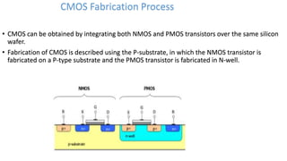
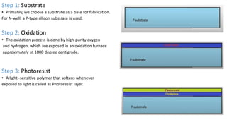
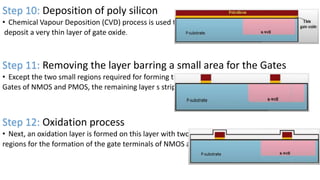
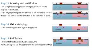
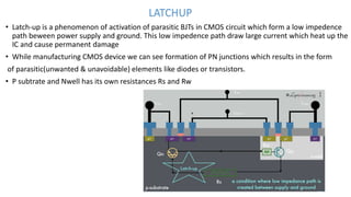
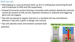
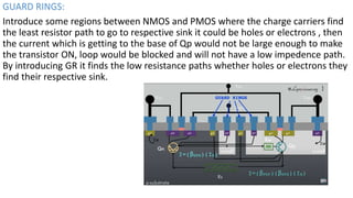
The document discusses the CMOS fabrication process using an N-well and describes steps to prevent latchup. It describes how parasitic BJTs can form a low impedance path between power and ground during CMOS fabrication. Key steps include depositing a P-type substrate, forming an N-well through diffusion, and adding well taps and guard rings to reduce substrate and well resistances to prevent triggering of the parasitic BJTs.