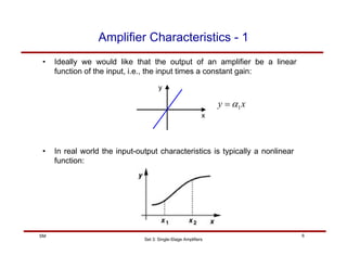
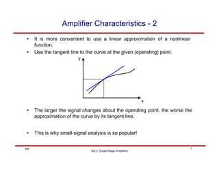
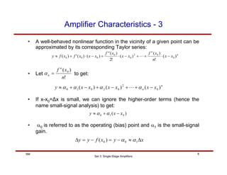
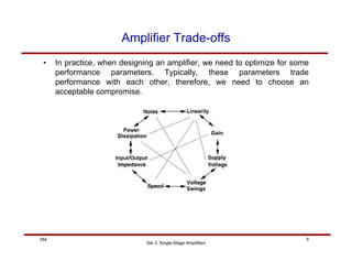
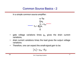
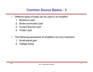
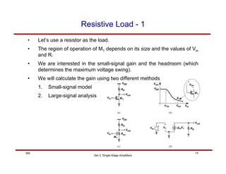
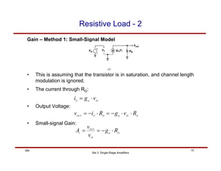
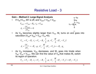
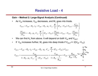
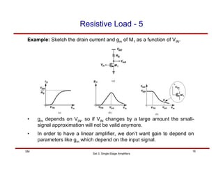
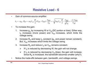
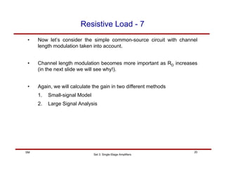
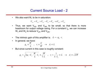
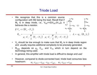
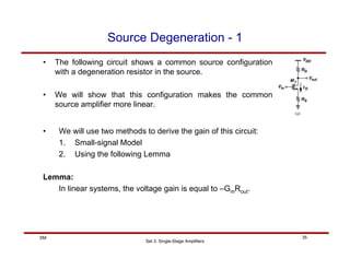
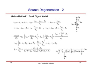
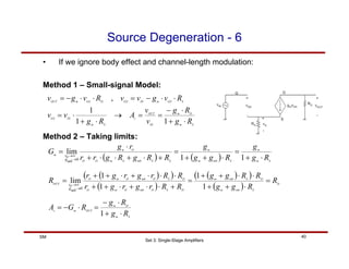
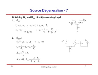
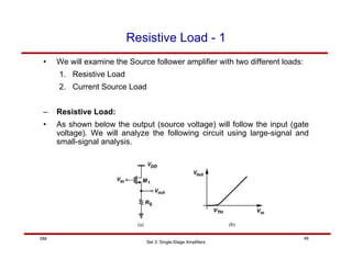
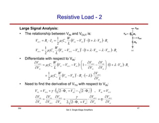
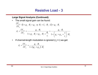
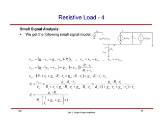
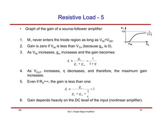
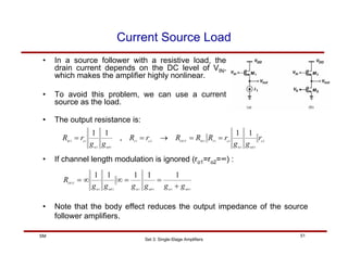
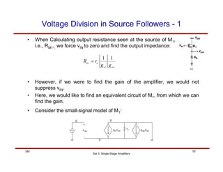
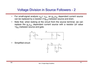
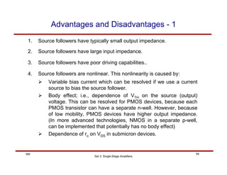
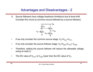
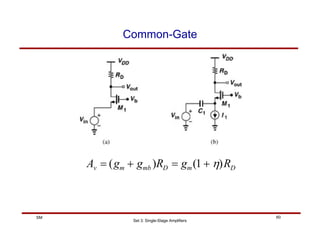
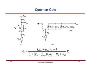
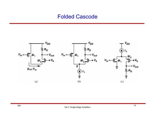
The document discusses single-stage amplifiers, specifically common source amplifiers. It covers the basics of common source amplifiers and different types of loads that can be used, including resistive loads. It analyzes the gain of common source amplifiers with resistive loads using both small-signal and large-signal models, taking into account effects such as channel length modulation. The analysis shows tradeoffs between gain, bandwidth, and voltage swing that must be considered in amplifier design.

![Set 3: Single-Stage Amplifiers
37
SM
Source Degeneration - 3
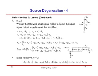
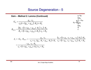
Gain – Method 2: Lemma
• The Lemma states that in linear systems, the voltage gain is
equal to –GmRout. So we need to find Gm and Rout.
1. Gm:
Recall that the equivalent transconductance of the above
Circuit is:
( ) ( ) S
S
mb
m
m
S
S
mb
S
m
m
m
R
R
g
g
r
r
g
R
R
g
R
g
r
r
r
g
v
i
G
O
O
O
O
O
IN
OUT
+
⋅
+
+
⋅
=
+
⋅
+
⋅
⋅
+
⋅
=
=
]
1
[](https://image.slidesharecdn.com/4-220216171424/85/4-single-stage-amplifier-37-320.jpg)
![Set 3: Single-Stage Amplifiers
66
SM
Common-Gate Output Impedance
D
S
o
S
mb
m
out R
R
r
R
g
g
R ||
}
]
)
(
1
{[ +
+
+
=](https://image.slidesharecdn.com/4-220216171424/85/4-single-stage-amplifier-66-320.jpg)
![Set 3: Single-Stage Amplifiers
68
SM
Cascode Stage
D
o
o
mb
m
D
o
o
o
mb
m
out
R
r
r
g
g
R
r
r
r
g
g
R
||
]
)
[(
||
}
]
)
(
1
{[
2
1
2
2
1
2
1
2
2
+
≈
+
+
+
=
AV ≈ gm1{[ro1ro2 (gm2 + gmb2 )] || RD ]}
• Cascade of a common-source stage and a common-gate stage is called a “cascode” stage.](https://image.slidesharecdn.com/4-220216171424/85/4-single-stage-amplifier-68-320.jpg)
![Set 3: Single-Stage Amplifiers
69
SM
Cascode Stage
AV ≈ gm1[(ro1ro2 gm2 ) || (ro3ro4gm3 )]](https://image.slidesharecdn.com/4-220216171424/85/4-single-stage-amplifier-69-320.jpg)


(
1
[ o
o
o
o
mb
m
out r
r
r
r
g
g
R +
+
+
=](https://image.slidesharecdn.com/4-220216171424/85/4-single-stage-amplifier-75-320.jpg)


