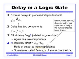
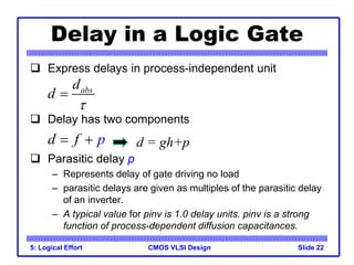
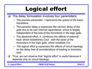
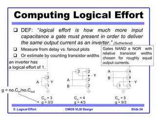
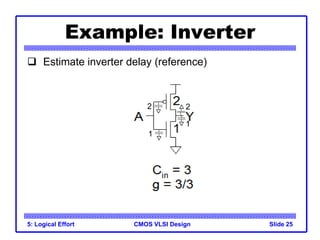
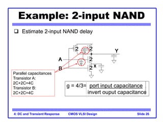
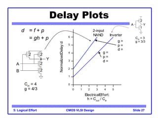
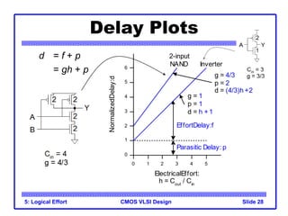
Introduction to
CMOS VLSI
Design
Lecture 5:
Logical Effort
GRECO-CIn-UFPE
Harvey Mudd College
Spring 2004
CMOS VLSI Design
5: Logical Effort Slide 2
Outline
 Introduction
 Delay in a Logic Gate
 Multistage Logic Networks
 Choosing the Best Number of Stages
 Example
 Summary
CMOS VLSI Design
5: Logical Effort Slide 3
Introduction
 Chip designers face a bewildering array of choices
– What is the best circuit topology for a function?
– How many stages of logic give least delay?
– How wide should the transistors be?
 Logical effort is a method to make these decisions
– Uses a simple model of delay
– Allows back-of-the-envelope calculations
– Helps make rapid comparisons between alternatives
– Emphasizes remarkable symmetries
? ? ?
CMOS VLSI Design
Logic effort
 The method of Logical effort is a easy way to
estimate delay in a CMOS circuit.
– We can select the fastest candidate by comparing
delay estimates of different logic structures.
– The method can specify the proper number of
logic stages.
– The method allows a early evaluation of the
design and provides a good starting point for
further optimizations.
5: Logical Effort Slide 4
CMOS VLSI Design
5: Logical Effort Slide 5
Chip design flow
CMOS VLSI Design
Technology dependency
Design levels
IBM
Technology dependence
Technology independency
CMOS VLSI Design
Circuit design styles
5: Logical Effort Slide 7
 Custom design
 Automatic design
CMOS VLSI Design
5: Logical Effort Slide 8
Custom design flow
 Additional human labor for better performance
- Designer has the flexibility to create cells at a transistor level
- Or choose from a library of predefined cells.
- Which technology?
- Static CMOS
- Transmission gate
- Domino circuit
- Any other logic family
- Which topology?
- NAND, NOR, INV or complex gates
- Size transistors of the logic gates
CMOS VLSI Design
5: Logical Effort Slide 9
Automatic design flow
 This method uses synthesis tools to choose circuit
topologies and gate sizes.
- Synthesis takes much less time than manually optimizing
paths and drawing schematics, but is generally restricted to
a fixed library of static CMOS cell.
- In general this method produces slower circuits than
designed by a skilled designer.
- Synthesized circuits are normally logically correct by
construction, but timing verification is still necessary.
- Performance can be improved by setting directives for
synthesis tool in order to solve critical paths delay.
CMOS VLSI Design
layout process
IBM
CMOS VLSI Design
Layout process
IBM
RC = Resistance
CAP = Capacitance
SDF = Standard Delay File
LVS
DRC
Antenna
Simulate and tweak
Making changes in a
circuit, throwing it into
the simulator, looking
at the result, making
more changes, and
repeating the process.
CMOS VLSI Design
Delay estimate
5: Logical Effort Slide 12
 The target her is design of fast chips.
- Use a systematic approach to topology selection and gate
sizing;
- A simple delay model that’s fast and easy to use.
- The delay model should be accurate enough that if it predicts
circuit a is significantly faster than circuit b, then circuit a
really is faster.
 Delay model
- Complexity of the gate;
- the load capacitance;
- parasitic capacitance.
CMOS VLSI Design
Delay model
5: Logical Effort Slide 13
 The delay model introduces a numeric “path effort”
that allows the designer to compare two multistage
topologies easily without sizing or simulation.
 The model allows choosing the best number of
stages of gates and for selecting each gate size in
order to minimize delay.
CMOS VLSI Design
Delay in a gate
5: Logical Effort Slide 14
 The model describes delays caused by the capacitive load
that the logic gate drives and by the topology of the logic gate.
 Clearly, as the load increases, the delay increases, but delay
also depends on the logic function of the gate.
2 2
1
1
Inverters, the simplest logic gates, drive loads
best and are often used as amplifiers to drive
large capacitances.
CMOS VLSI Design
5: Logical Effort Slide 15
Logic gates that compute other functions
require more transistors, some of which are
connected in series, making them
poorer than inverters at driving current.
Delay in logic gates
A NAND gate has more delay than a inverter with
similar transistor sizes that drives the same load.
A 2-input NAND gate
CMOS VLSI Design
 To model the delay if a logic gate
– Firstly, to isolate the effects of a particular
integrated circuit fabrication process by expressing
all delays in terms of a basic “unit  “ particular to
that process.
–  is the delay of an inverter driving an identical
inverter with no parasitics.
– Thus we express absolute delay as the product of a
unitless delay of the gate d and the delay unit that
characterizes a given process:
Slide 16
Delay in a Logic Gate
CMOS VLSI Design
5: Logical Effort Slide 17
Delay in a Logic Gate
 Express delays in process-independent unit
abs
d
d


  3RC
 12 ps in 180 nm process
40 ps in 0.6 mm process
CMOS VLSI Design
5: Logical Effort Slide 18
Delay in a Logic Gate
 Express delays in process-independent unit
 Delay has two components
abs
d
d


d f p
 
CMOS VLSI Design
5: Logical Effort Slide 19
Delay in a Logic Gate
 Express delays in process-independent unit
 Delay has two components
 Effort delay f = gh (proportional to the load on the
gate’s output)
– Again has two components
– The effort delay depends on the load and on
properties of the logic gate driving the load.
abs
d
d


d p
f
 
CMOS VLSI Design
5: Logical Effort Slide 20
Delay in a Logic Gate
 Express delays in process-independent unit
 Delay has two components
 Effort delay f = gh (related to gate’s load)
– Again has two components
 g: logical effort (g is determined by gate’s structure)
– g captures properties of the logic gate,
– g  1 for inverter
abs
d
d


d f p
 
CMOS VLSI Design
5: Logical Effort Slide 21
Delay in a Logic Gate
 Express delays in process-independent unit
 Delay has two components
 Effort delay f = gh (related to gate’s load)
– Again has two components
 h: electrical effort = Cout / Cin
– Ratio of output to input capacitance
– Sometimes called fanout, h characterizes the load
abs
d
d


d f p
 
fanout, in this context,
depends on the load
capacitance, not just
the number of gates
being driven.
CMOS VLSI Design
5: Logical Effort Slide 22
Delay in a Logic Gate
 Express delays in process-independent unit
 Delay has two components
 Parasitic delay p
– Represents delay of gate driving no load
– parasitic delays are given as multiples of the parasitic delay
of an inverter.
– A typical value for pinv is 1.0 delay units. pinv is a strong
function of process-dependent diffusion capacitances.
abs
d
d


d p
f
  d = gh+p
CMOS VLSI Design
Logical effort
 The delay formulation involves four parameters:
– The process parameter  represents the speed of the basic
transistors.
– The parasitic delay p expresses the intrinsic delay of the
gate due to its own internal capacitance, which is largely
independent of the size of the transistors in the logic gate.
– The electrical effort, h, combines the effects of external
load, which establishes Cout , with the sizes of the
transistors in the logic gate, which establish Cin.
– The logical effort g expresses the effects of circuit topology
on the delay free of considerations of loading or transistor
size.
 Thus, we can observe that “logical effort” is useful because it
depends only on circuit topology.
5: Logical Effort Slide 23
CMOS VLSI Design
5: Logical Effort Slide 24
Computing Logical Effort
 DEF: “logical effort is how much more input
capacitance a gate must present in order to deliver
the same output current as an inverter.” (Sutherland)
 Measure from delay vs. fanout plots
 Or estimate by counting transistor widths
A Y
A
B
Y
A
B
Y
1
2
1 1
2 2
2
2
4
4
Cin
= 3
g = 3/3
Cin
= 4
g = 4/3
Cin
= 5
g = 5/3
an inverter has
a logical effort of 1.
Gates NAND e NOR with
relative transistor widths
chosen for roughly equal
output currents.
g = no.Cin/no.Cout
CMOS VLSI Design
5: Logical Effort Slide 25
Example: Inverter
 Estimate inverter delay (reference)
2 2
1
1
CMOS VLSI Design
4: DC and Transient Response Slide 26
Example: 2-input NAND
 Estimate 2-input NAND delay
Parallel capacitances
Transistor A:
2C+2C=4C
Transistor B:
2C+2C=4C
g = 4/3= port input capacitance
invert ouput capacitance
CMOS VLSI Design
5: Logical Effort Slide 27
Delay Plots
d = f + p
= gh + p
ElectricalEffort:
h = Cout
/ Cin
Normalized
Delay:
d
Inverter
2-input
NAND
g =
p =
d =
g =
p =
d =
0 1 2 3 4 5
0
1
2
3
4
5
6
CMOS VLSI Design
5: Logical Effort Slide 28
Delay Plots
d = f + p
= gh + p
ElectricalEffort:
h = Cout
/ Cin
Normalized
Delay:
d
Inverter
2-input
NAND
g = 1
p = 1
d = h +1
g = 4/3
p = 2
d = (4/3)h +2
EffortDelay:f
Parasitic Delay: p
0 1 2 3 4 5
0
1
2
3
4
5
6
CMOS VLSI Design
5: Logical Effort Slide 29
Catalog of Gates
Gate type Number of inputs
1 2 3 4 n
Inverter 1
NAND 4/3 5/3 6/3 (n+2)/3
NOR 5/3 7/3 9/3 (2n+1)/3
Tristate / mux 2 2 2 2 2
XOR, XNOR 4, 4 6, 12, 6 8, 16, 16, 8
 Logical effort of common gates
CMOS VLSI Design
30
Example – 8-input AND
CMOS VLSI Design
5: Logical Effort Slide 31
Catalog of Gates
Gate type Number of inputs
1 2 3 4 n
Inverter 1
NAND 2 3 4 n
NOR 2 3 4 n
Tristate / mux 2 4 6 8 2n
XOR, XNOR 4 6 8
 Parasitic delay of common gates
– In multiples of pinv (1)

lect501.ppt

  • 1.
    Introduction to CMOS VLSI Design Lecture5: Logical Effort GRECO-CIn-UFPE Harvey Mudd College Spring 2004
  • 2.
    CMOS VLSI Design 5:Logical Effort Slide 2 Outline  Introduction  Delay in a Logic Gate  Multistage Logic Networks  Choosing the Best Number of Stages  Example  Summary
  • 3.
    CMOS VLSI Design 5:Logical Effort Slide 3 Introduction  Chip designers face a bewildering array of choices – What is the best circuit topology for a function? – How many stages of logic give least delay? – How wide should the transistors be?  Logical effort is a method to make these decisions – Uses a simple model of delay – Allows back-of-the-envelope calculations – Helps make rapid comparisons between alternatives – Emphasizes remarkable symmetries ? ? ?
  • 4.
    CMOS VLSI Design Logiceffort  The method of Logical effort is a easy way to estimate delay in a CMOS circuit. – We can select the fastest candidate by comparing delay estimates of different logic structures. – The method can specify the proper number of logic stages. – The method allows a early evaluation of the design and provides a good starting point for further optimizations. 5: Logical Effort Slide 4
  • 5.
    CMOS VLSI Design 5:Logical Effort Slide 5 Chip design flow
  • 6.
    CMOS VLSI Design Technologydependency Design levels IBM Technology dependence Technology independency
  • 7.
    CMOS VLSI Design Circuitdesign styles 5: Logical Effort Slide 7  Custom design  Automatic design
  • 8.
    CMOS VLSI Design 5:Logical Effort Slide 8 Custom design flow  Additional human labor for better performance - Designer has the flexibility to create cells at a transistor level - Or choose from a library of predefined cells. - Which technology? - Static CMOS - Transmission gate - Domino circuit - Any other logic family - Which topology? - NAND, NOR, INV or complex gates - Size transistors of the logic gates
  • 9.
    CMOS VLSI Design 5:Logical Effort Slide 9 Automatic design flow  This method uses synthesis tools to choose circuit topologies and gate sizes. - Synthesis takes much less time than manually optimizing paths and drawing schematics, but is generally restricted to a fixed library of static CMOS cell. - In general this method produces slower circuits than designed by a skilled designer. - Synthesized circuits are normally logically correct by construction, but timing verification is still necessary. - Performance can be improved by setting directives for synthesis tool in order to solve critical paths delay.
  • 10.
  • 11.
    CMOS VLSI Design Layoutprocess IBM RC = Resistance CAP = Capacitance SDF = Standard Delay File LVS DRC Antenna Simulate and tweak Making changes in a circuit, throwing it into the simulator, looking at the result, making more changes, and repeating the process.
  • 12.
    CMOS VLSI Design Delayestimate 5: Logical Effort Slide 12  The target her is design of fast chips. - Use a systematic approach to topology selection and gate sizing; - A simple delay model that’s fast and easy to use. - The delay model should be accurate enough that if it predicts circuit a is significantly faster than circuit b, then circuit a really is faster.  Delay model - Complexity of the gate; - the load capacitance; - parasitic capacitance.
  • 13.
    CMOS VLSI Design Delaymodel 5: Logical Effort Slide 13  The delay model introduces a numeric “path effort” that allows the designer to compare two multistage topologies easily without sizing or simulation.  The model allows choosing the best number of stages of gates and for selecting each gate size in order to minimize delay.
  • 14.
    CMOS VLSI Design Delayin a gate 5: Logical Effort Slide 14  The model describes delays caused by the capacitive load that the logic gate drives and by the topology of the logic gate.  Clearly, as the load increases, the delay increases, but delay also depends on the logic function of the gate. 2 2 1 1 Inverters, the simplest logic gates, drive loads best and are often used as amplifiers to drive large capacitances.
  • 15.
    CMOS VLSI Design 5:Logical Effort Slide 15 Logic gates that compute other functions require more transistors, some of which are connected in series, making them poorer than inverters at driving current. Delay in logic gates A NAND gate has more delay than a inverter with similar transistor sizes that drives the same load. A 2-input NAND gate
  • 16.
    CMOS VLSI Design To model the delay if a logic gate – Firstly, to isolate the effects of a particular integrated circuit fabrication process by expressing all delays in terms of a basic “unit  “ particular to that process. –  is the delay of an inverter driving an identical inverter with no parasitics. – Thus we express absolute delay as the product of a unitless delay of the gate d and the delay unit that characterizes a given process: Slide 16 Delay in a Logic Gate
  • 17.
    CMOS VLSI Design 5:Logical Effort Slide 17 Delay in a Logic Gate  Express delays in process-independent unit abs d d     3RC  12 ps in 180 nm process 40 ps in 0.6 mm process
  • 18.
    CMOS VLSI Design 5:Logical Effort Slide 18 Delay in a Logic Gate  Express delays in process-independent unit  Delay has two components abs d d   d f p  
  • 19.
    CMOS VLSI Design 5:Logical Effort Slide 19 Delay in a Logic Gate  Express delays in process-independent unit  Delay has two components  Effort delay f = gh (proportional to the load on the gate’s output) – Again has two components – The effort delay depends on the load and on properties of the logic gate driving the load. abs d d   d p f  
  • 20.
    CMOS VLSI Design 5:Logical Effort Slide 20 Delay in a Logic Gate  Express delays in process-independent unit  Delay has two components  Effort delay f = gh (related to gate’s load) – Again has two components  g: logical effort (g is determined by gate’s structure) – g captures properties of the logic gate, – g  1 for inverter abs d d   d f p  
  • 21.
    CMOS VLSI Design 5:Logical Effort Slide 21 Delay in a Logic Gate  Express delays in process-independent unit  Delay has two components  Effort delay f = gh (related to gate’s load) – Again has two components  h: electrical effort = Cout / Cin – Ratio of output to input capacitance – Sometimes called fanout, h characterizes the load abs d d   d f p   fanout, in this context, depends on the load capacitance, not just the number of gates being driven.
  • 22.
    CMOS VLSI Design 5:Logical Effort Slide 22 Delay in a Logic Gate  Express delays in process-independent unit  Delay has two components  Parasitic delay p – Represents delay of gate driving no load – parasitic delays are given as multiples of the parasitic delay of an inverter. – A typical value for pinv is 1.0 delay units. pinv is a strong function of process-dependent diffusion capacitances. abs d d   d p f   d = gh+p
  • 23.
    CMOS VLSI Design Logicaleffort  The delay formulation involves four parameters: – The process parameter  represents the speed of the basic transistors. – The parasitic delay p expresses the intrinsic delay of the gate due to its own internal capacitance, which is largely independent of the size of the transistors in the logic gate. – The electrical effort, h, combines the effects of external load, which establishes Cout , with the sizes of the transistors in the logic gate, which establish Cin. – The logical effort g expresses the effects of circuit topology on the delay free of considerations of loading or transistor size.  Thus, we can observe that “logical effort” is useful because it depends only on circuit topology. 5: Logical Effort Slide 23
  • 24.
    CMOS VLSI Design 5:Logical Effort Slide 24 Computing Logical Effort  DEF: “logical effort is how much more input capacitance a gate must present in order to deliver the same output current as an inverter.” (Sutherland)  Measure from delay vs. fanout plots  Or estimate by counting transistor widths A Y A B Y A B Y 1 2 1 1 2 2 2 2 4 4 Cin = 3 g = 3/3 Cin = 4 g = 4/3 Cin = 5 g = 5/3 an inverter has a logical effort of 1. Gates NAND e NOR with relative transistor widths chosen for roughly equal output currents. g = no.Cin/no.Cout
  • 25.
    CMOS VLSI Design 5:Logical Effort Slide 25 Example: Inverter  Estimate inverter delay (reference) 2 2 1 1
  • 26.
    CMOS VLSI Design 4:DC and Transient Response Slide 26 Example: 2-input NAND  Estimate 2-input NAND delay Parallel capacitances Transistor A: 2C+2C=4C Transistor B: 2C+2C=4C g = 4/3= port input capacitance invert ouput capacitance
  • 27.
    CMOS VLSI Design 5:Logical Effort Slide 27 Delay Plots d = f + p = gh + p ElectricalEffort: h = Cout / Cin Normalized Delay: d Inverter 2-input NAND g = p = d = g = p = d = 0 1 2 3 4 5 0 1 2 3 4 5 6
  • 28.
    CMOS VLSI Design 5:Logical Effort Slide 28 Delay Plots d = f + p = gh + p ElectricalEffort: h = Cout / Cin Normalized Delay: d Inverter 2-input NAND g = 1 p = 1 d = h +1 g = 4/3 p = 2 d = (4/3)h +2 EffortDelay:f Parasitic Delay: p 0 1 2 3 4 5 0 1 2 3 4 5 6
  • 29.
    CMOS VLSI Design 5:Logical Effort Slide 29 Catalog of Gates Gate type Number of inputs 1 2 3 4 n Inverter 1 NAND 4/3 5/3 6/3 (n+2)/3 NOR 5/3 7/3 9/3 (2n+1)/3 Tristate / mux 2 2 2 2 2 XOR, XNOR 4, 4 6, 12, 6 8, 16, 16, 8  Logical effort of common gates
  • 30.
  • 31.
    CMOS VLSI Design 5:Logical Effort Slide 31 Catalog of Gates Gate type Number of inputs 1 2 3 4 n Inverter 1 NAND 2 3 4 n NOR 2 3 4 n Tristate / mux 2 4 6 8 2n XOR, XNOR 4 6 8  Parasitic delay of common gates – In multiples of pinv (1)

Editor's Notes