Downloaded 1,289 times

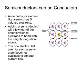
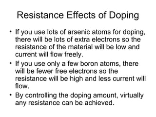
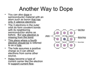
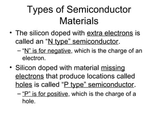
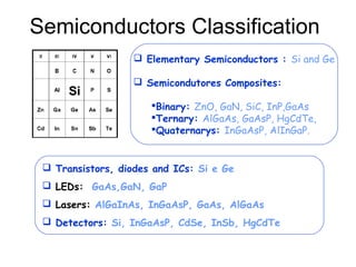
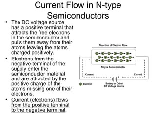
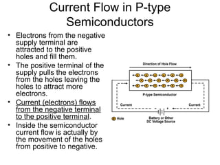
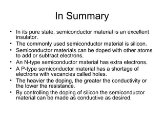

Semiconductor materials like silicon can be made to conduct electricity through "doping" with other atoms. Doping with atoms having extra electrons makes the material N-type and conductive, while doping with atoms missing electrons makes it P-type conductive. Semiconductor devices widely use controlled doping of silicon to generate and regulate electric current flow.


