Downloaded 415 times


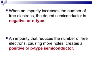
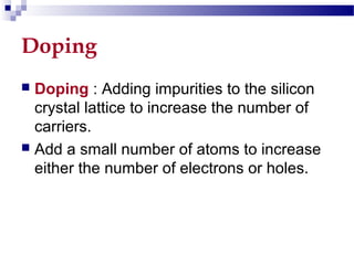
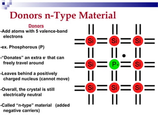
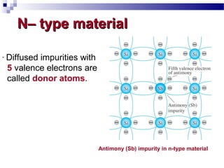

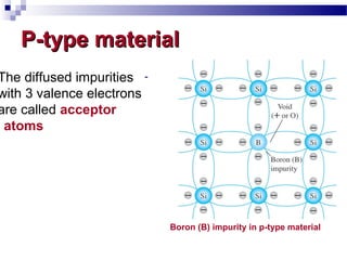
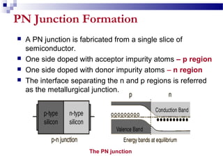
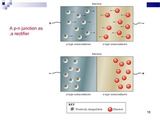

1) Semiconductors have two energy bands called the valence band and conduction band, separated by a forbidden gap. 2) They can be classified as intrinsic or extrinsic. Intrinsic semiconductors are pure, while extrinsic are doped with impurities to alter conductivity. 3) Doping a semiconductor by adding impurities that add free electrons makes it an n-type semiconductor, while adding impurities that add free holes makes it a p-type semiconductor. A p-n junction formed from a p-type and n-type semiconductor can function as a rectifier.


![Human Reproduction [ Reproductive System ] Notes @irfanullah_mehar Irfanullah...](https://cdn.slidesharecdn.com/ss_thumbnails/humanreproductionreproductivesystemnotesirfanullahmeharirfanullahmeharjanantantra-260111172350-56e85778-thumbnail.jpg?width=640&height=640&fit=bounds)


