Downloaded 2,361 times

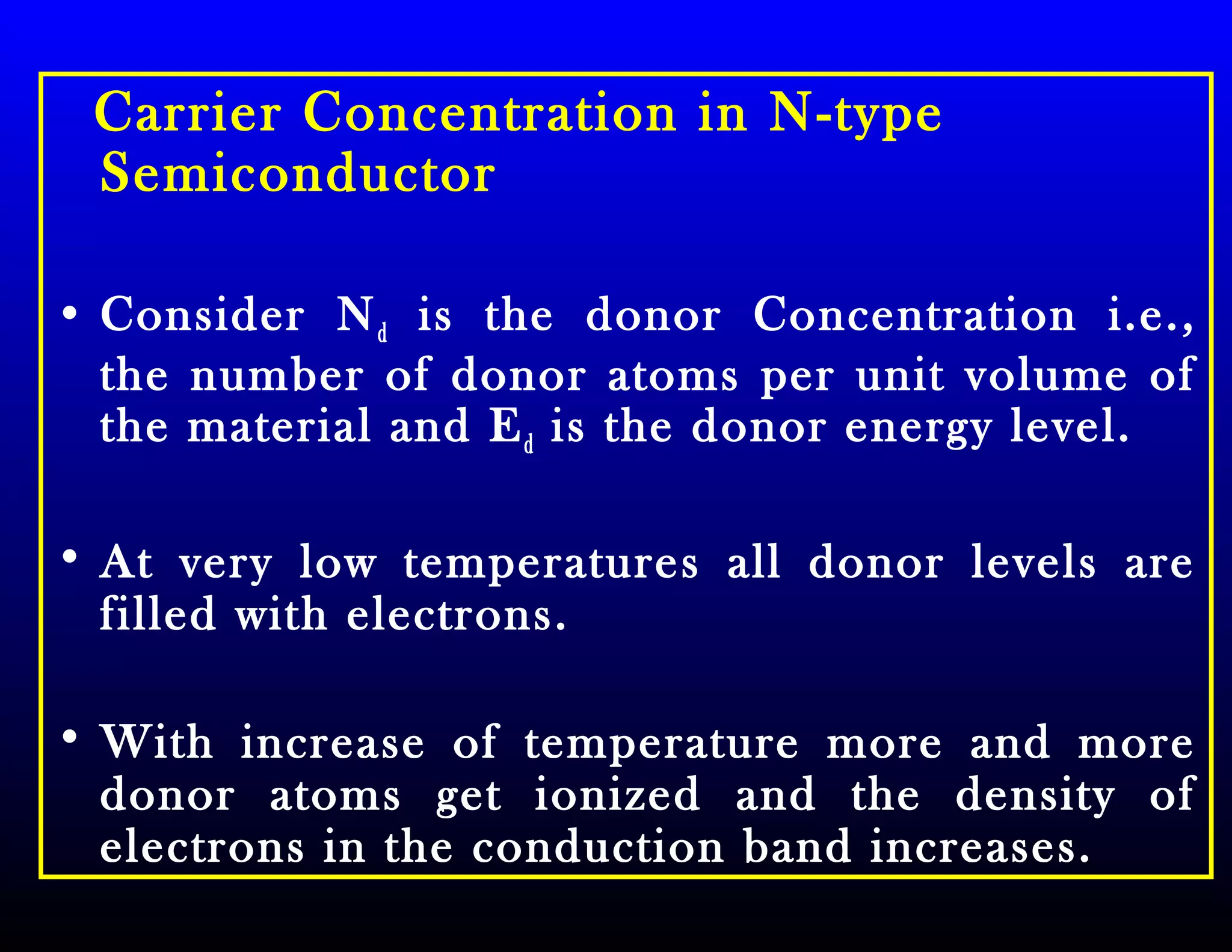
![Density of electrons in the Conduction band
kT
EE
h
kTm
N
kT
EE
h
kTm
N
kT
EE
kT
EE
kT
E
h
kTm
N
kT
EE
kT
EE
kT
E
h
kTm
NkTEE
kT
EE
kT
EE
h
kTm
n
cd
e
dcF
e
dcdcF
c
e
dcdcF
c
e
dcd
cF
cFe
2
)(
exp
])
2
(2[
)(
)exp(
}
])
2
(2[
)(
log
2
)(
exp{)exp(
}
])
2
(2[
)(
log
2
)(
exp{)exp(
}
}
)
2
(2
log
22
)(
{
exp{)exp(
)exp()
2
(2
2
1
2
1
2
1
2
3
2
2
1
2
3
2
2
1
2
3
2
2
1
2
3
2
2
3
2
−
=
−
+
−
=
−
−+
+
=
−
−+
+
=
−
−
=
∗
∗
∗
∗
∗
π
π
π
π
π](https://image.slidesharecdn.com/unit-1-140606230746-phpapp01/75/SEMICONDUCTOR-PHYSICS-33-2048.jpg)
![kT
EE
h
kTm
Nn
kT
EE
h
kTm
N
h
kTm
n
kT
EE
h
kTm
n
cde
d
cd
e
de
cFe
2
)(
exp)
2
()2(
}
2
)(
exp
])
2
(2[
)(
{)
2
(2
)exp()
2
(2
4
3
2
2
1
2
3
2
2
1
2
3
2
2
3
2
2
1
−
=
−
=
−
=
∗
∗
∗
∗
π
π
π
π
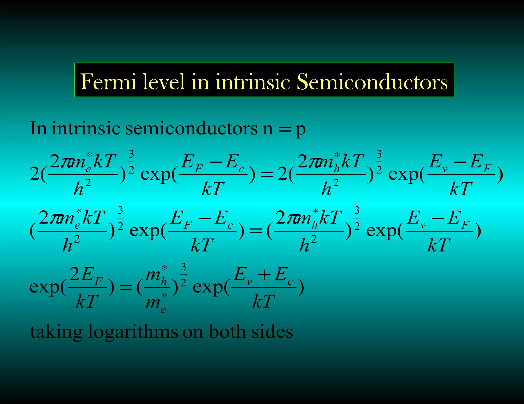
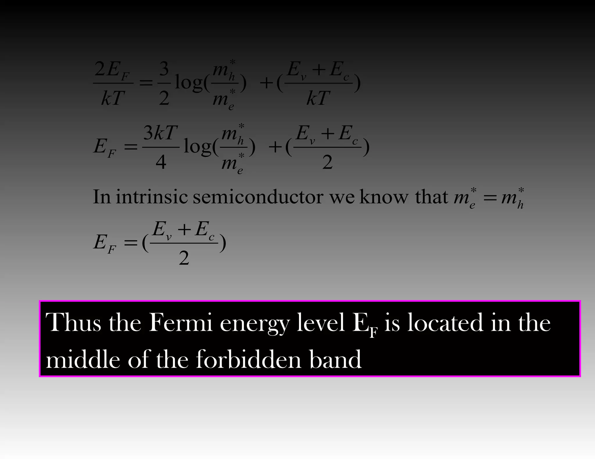
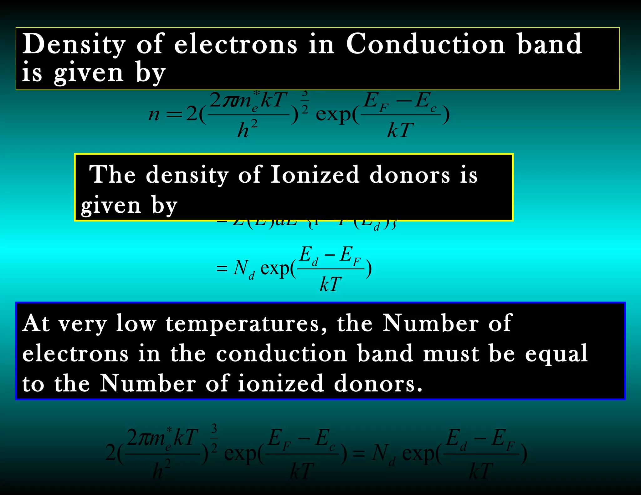
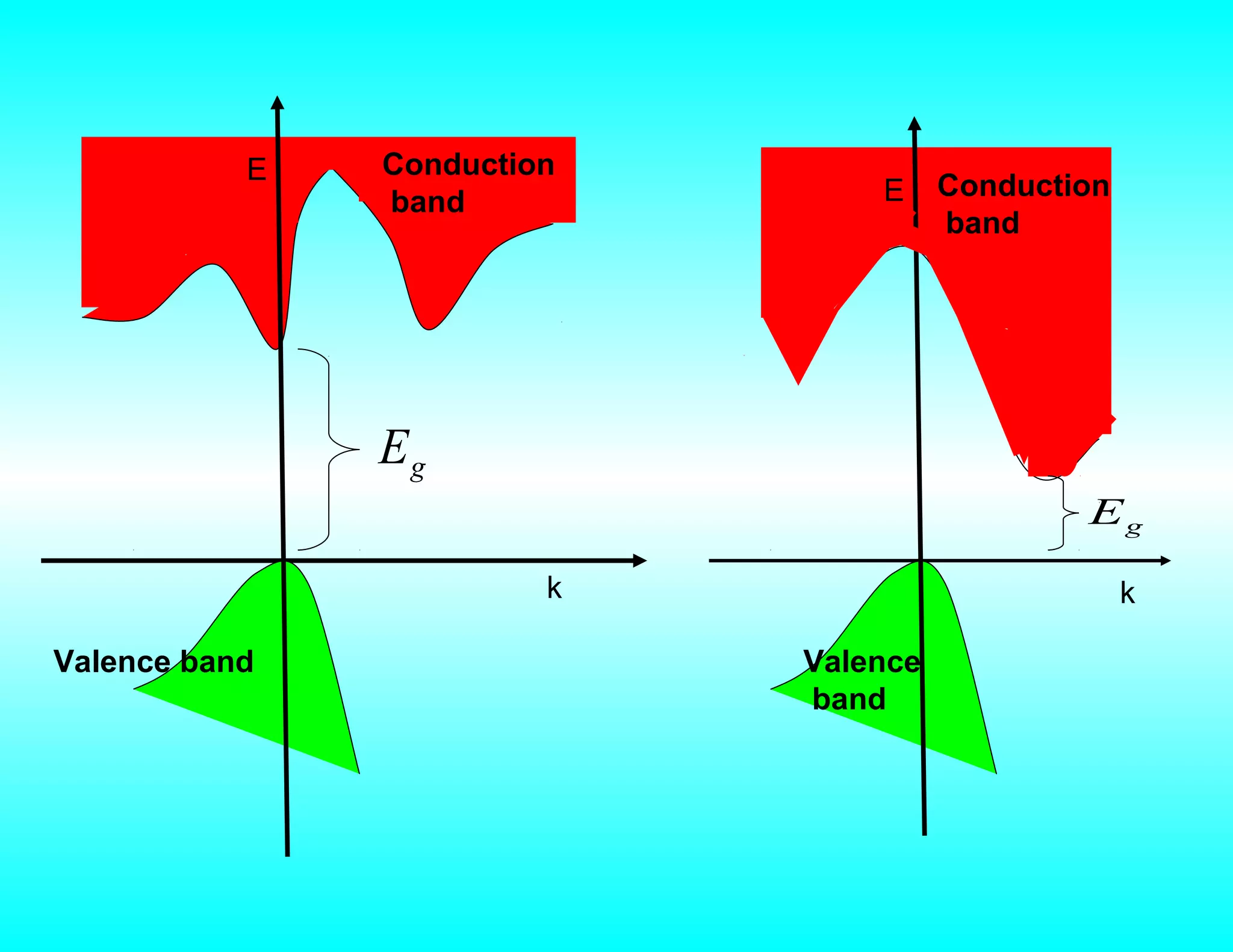
Thus we find that the density of electrons in the
conduction band is proportional to the square
root of the donor concentration at moderately low
temperatures.](https://image.slidesharecdn.com/unit-1-140606230746-phpapp01/75/SEMICONDUCTOR-PHYSICS-34-2048.jpg)
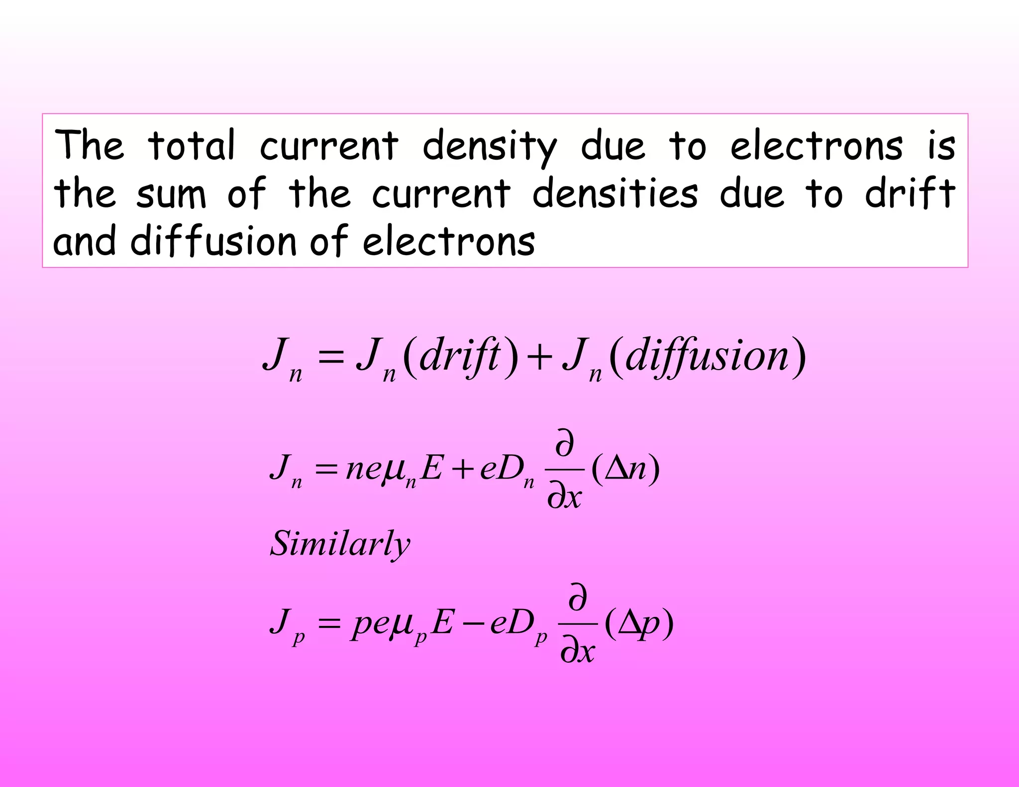
]([)( p
x
DediffusionJ pP ∆
∂
∂
−+=
)( p
x
eDp ∆
∂
∂
−=
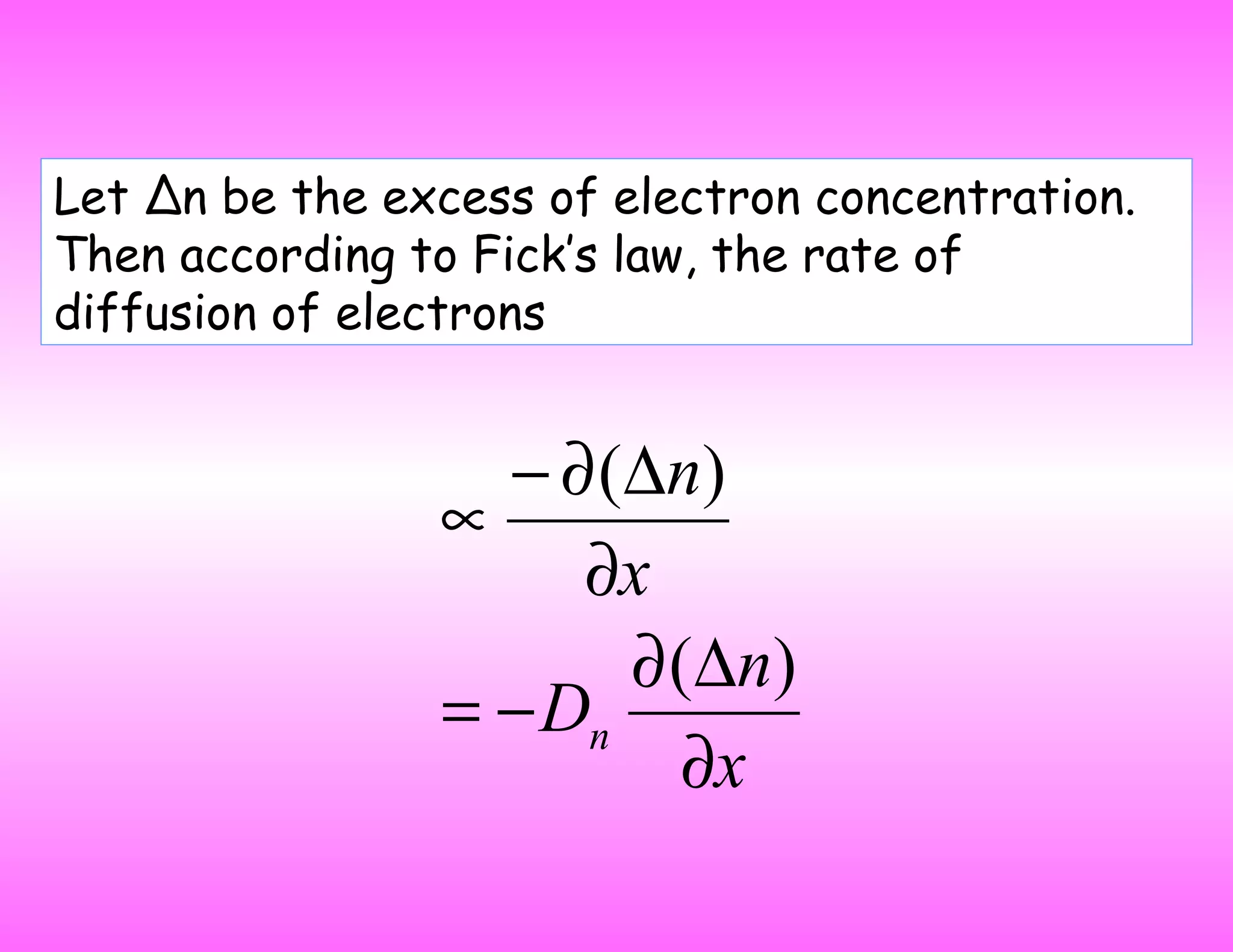
Where Dn is the diffusion of electrons, the
diffusion current density due to electrons is
given by Jn(diffusion)](https://image.slidesharecdn.com/unit-1-140606230746-phpapp01/75/SEMICONDUCTOR-PHYSICS-47-2048.jpg)

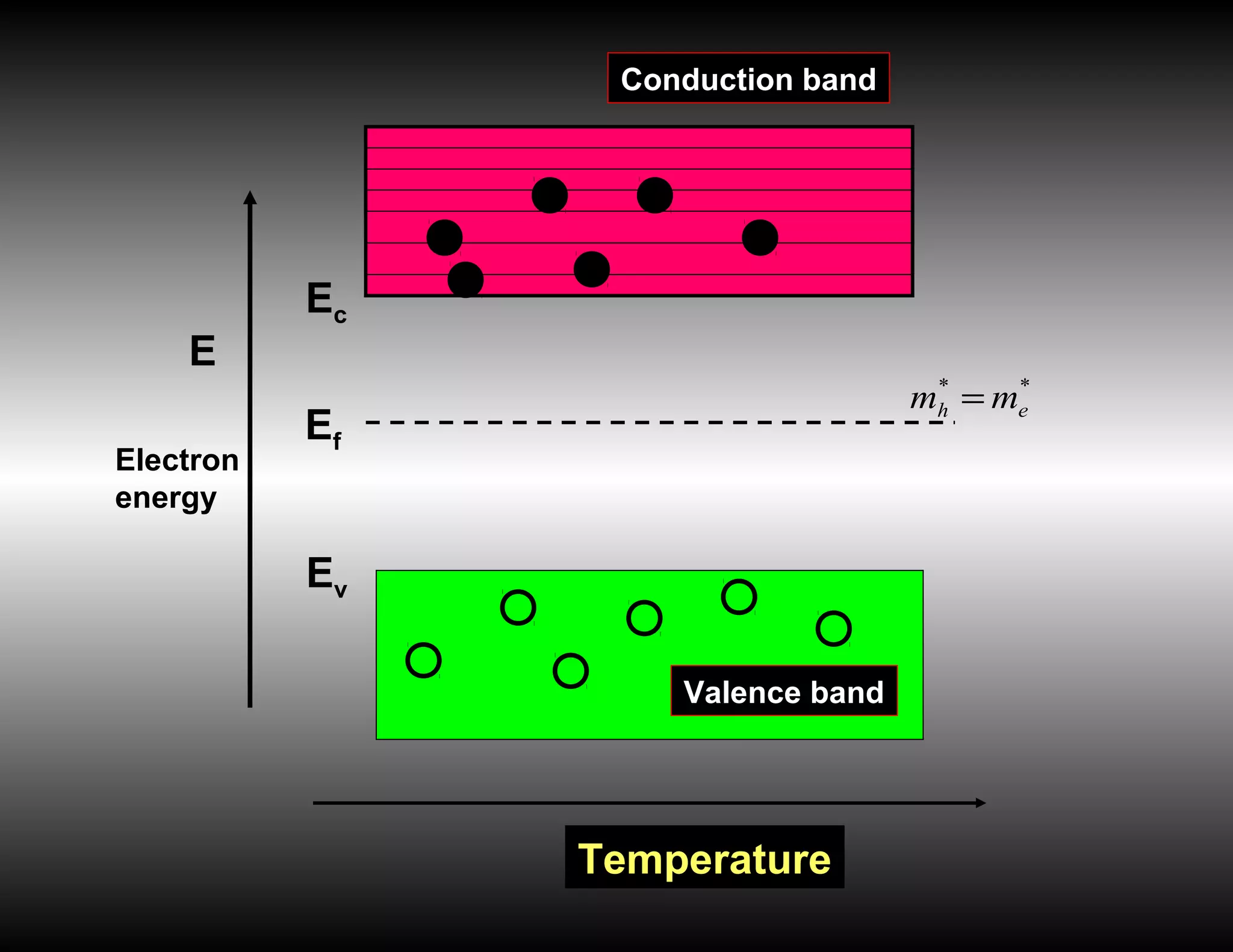
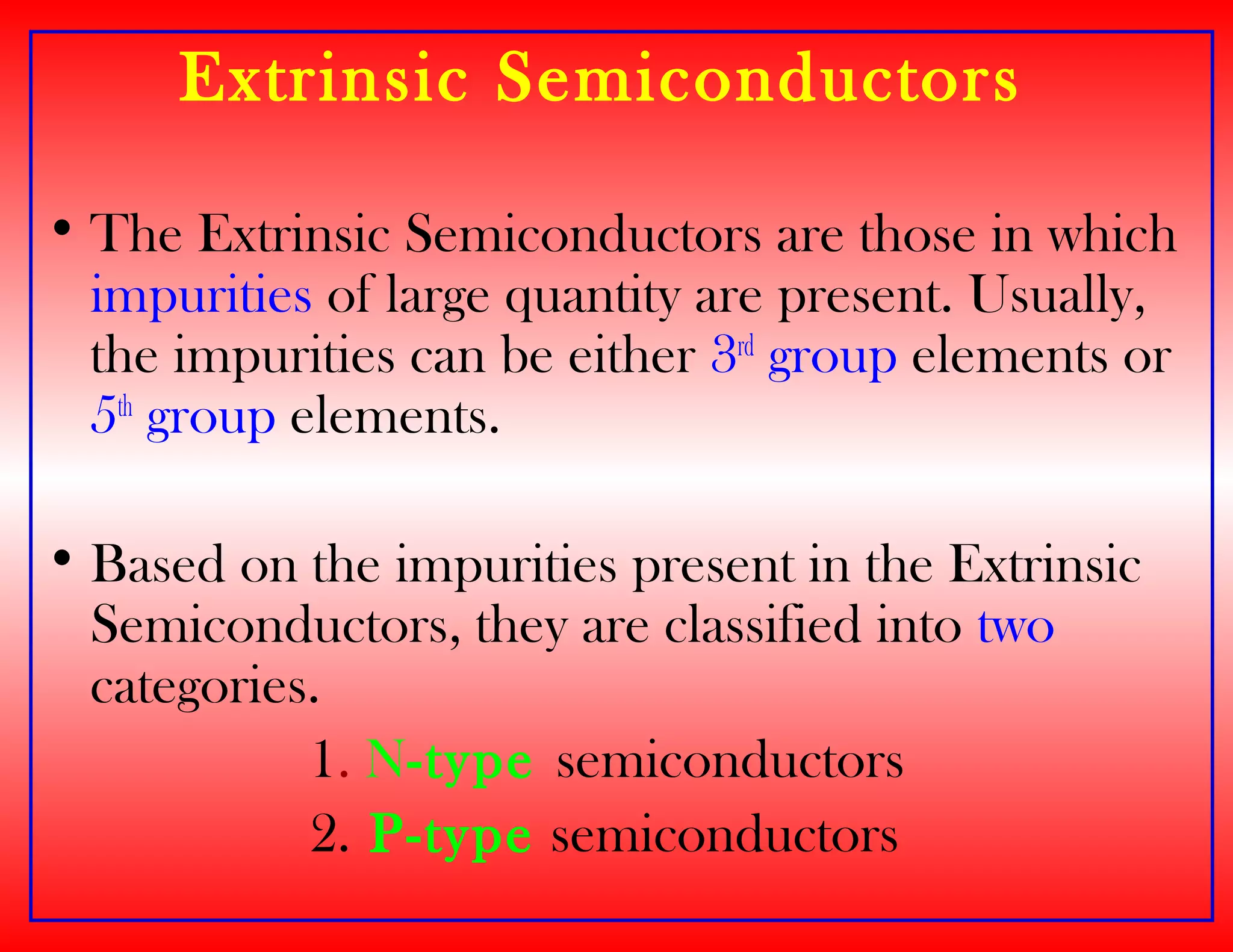
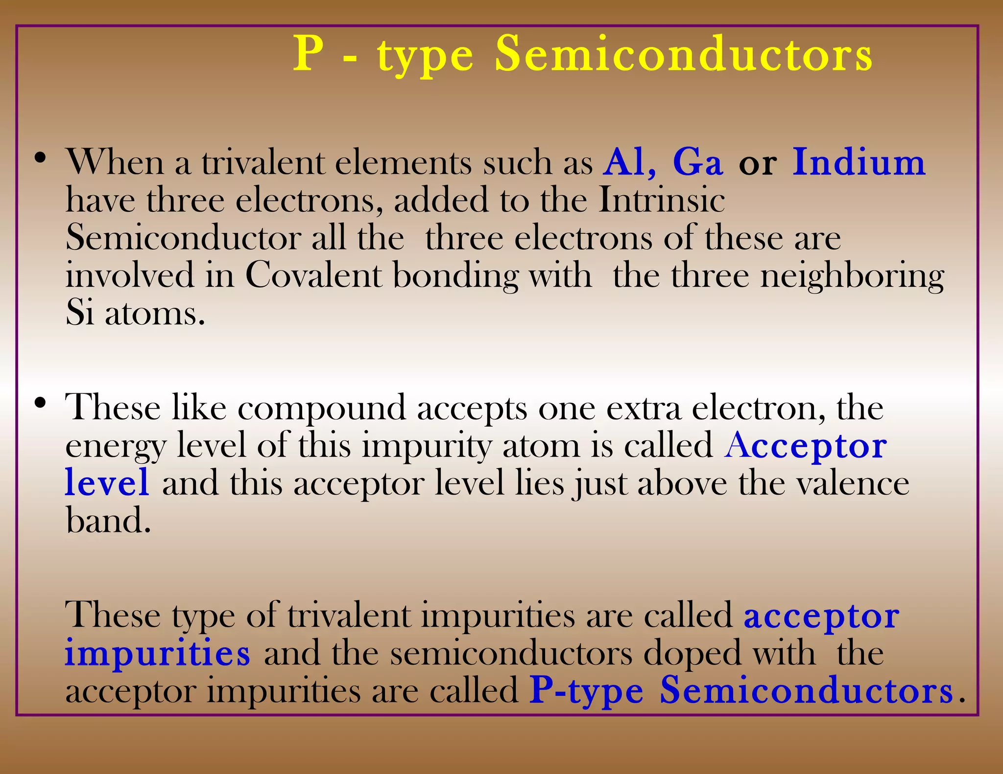
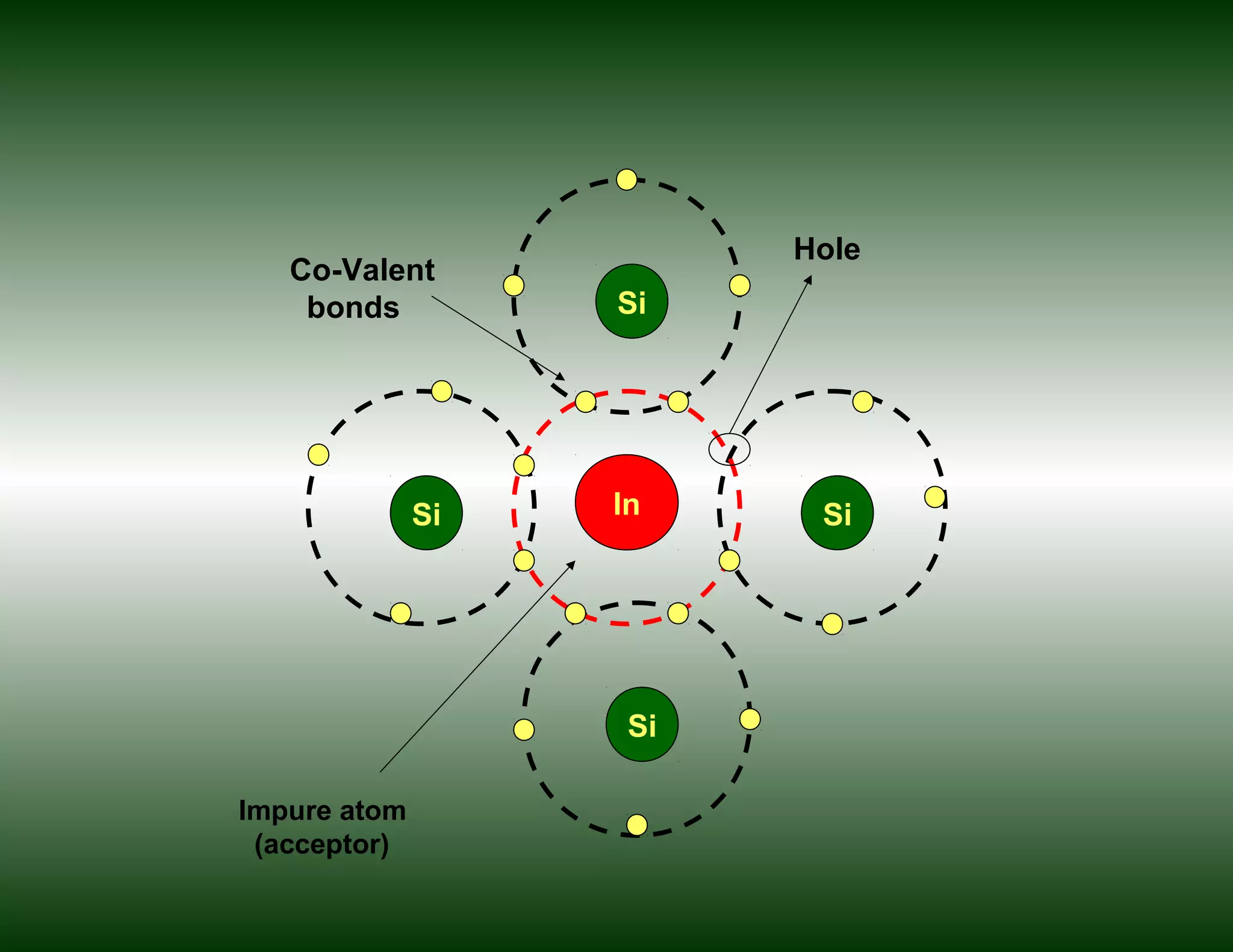
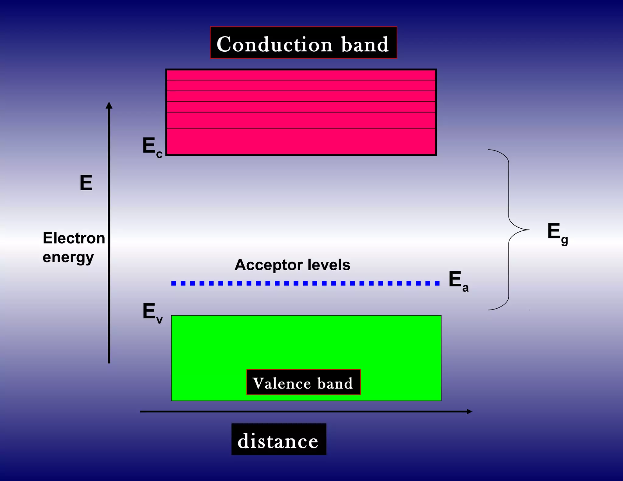
Semiconductor Physics In 3 sentences: Semiconductors have electrical properties between metals and insulators, with conductivities from 10-4 to 104 S/m. Their crystal structure leads to electrons being able to move between valence and conduction bands, making semiconductors bipolar with both electrons and holes conducting. Semiconductors are classified as intrinsic, with equal electron and hole concentrations determined by temperature, or extrinsic with additional carriers from dopant impurities making them either n-type or p-type.


