Downloaded 1,449 times


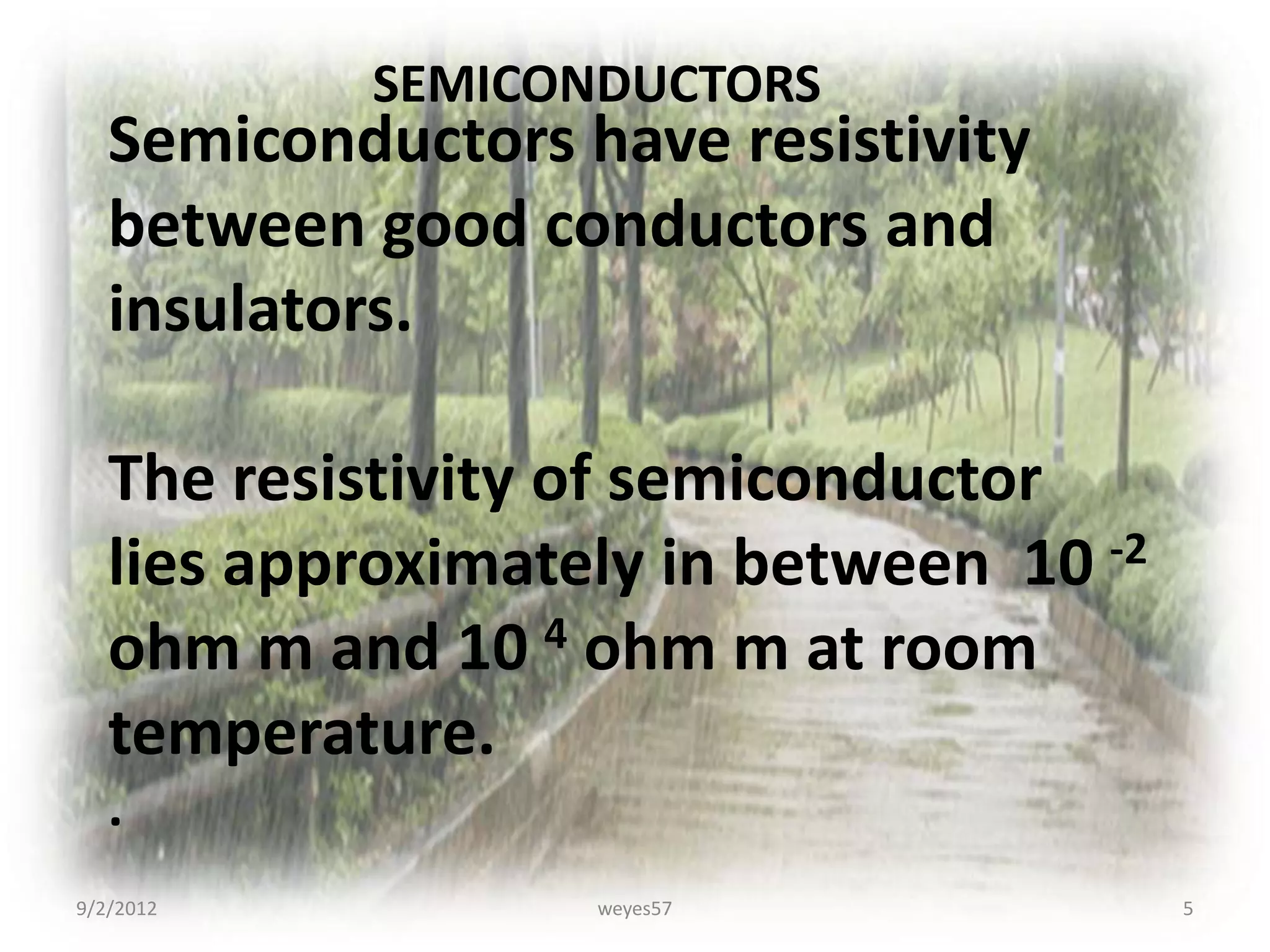
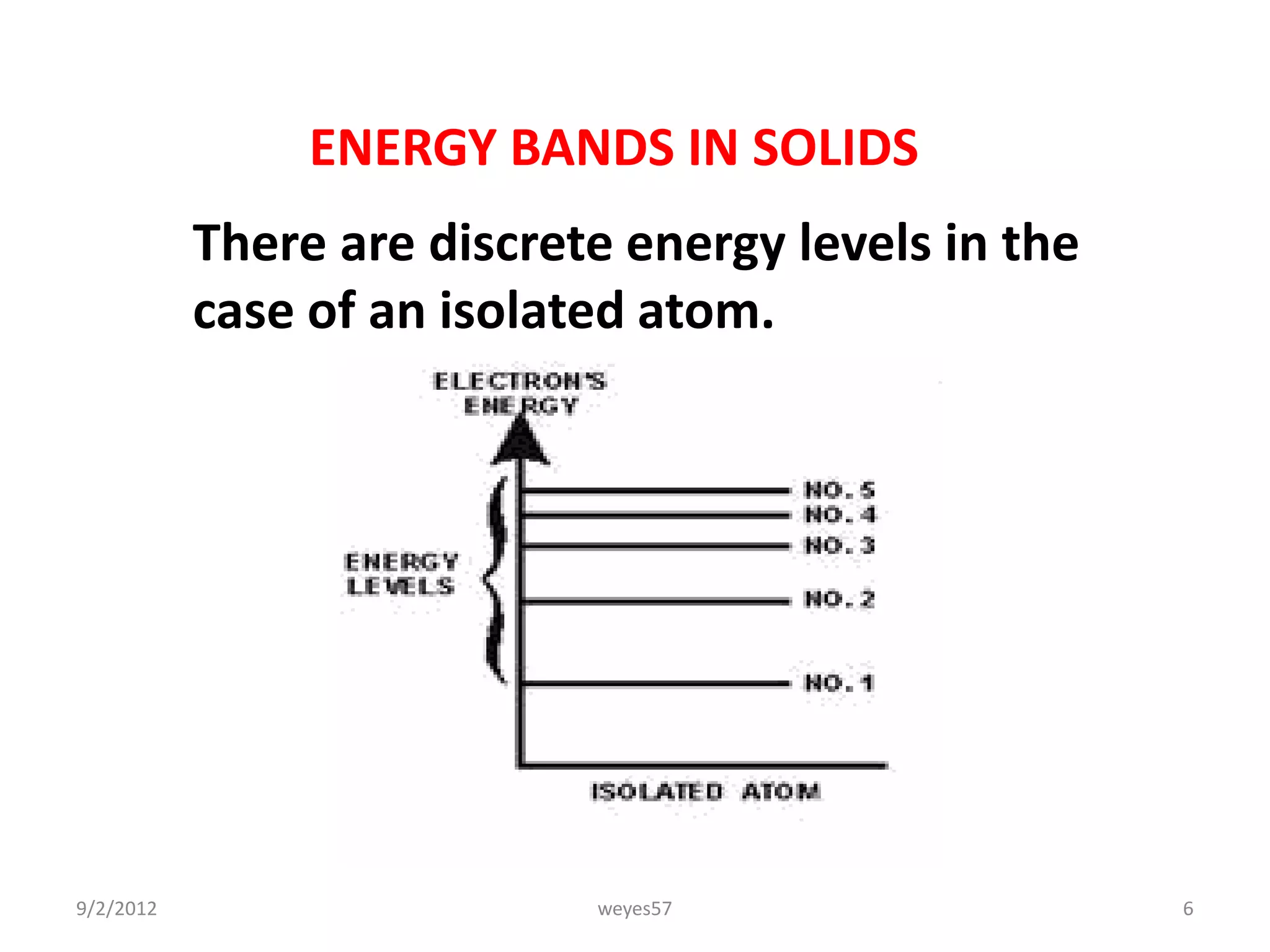
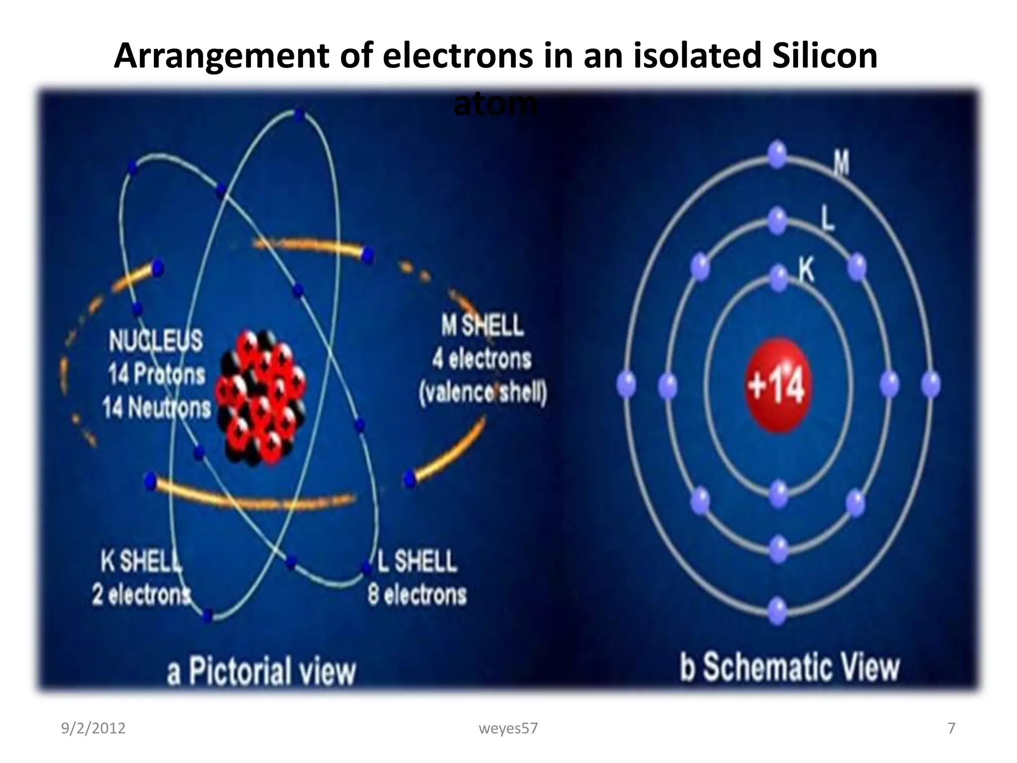
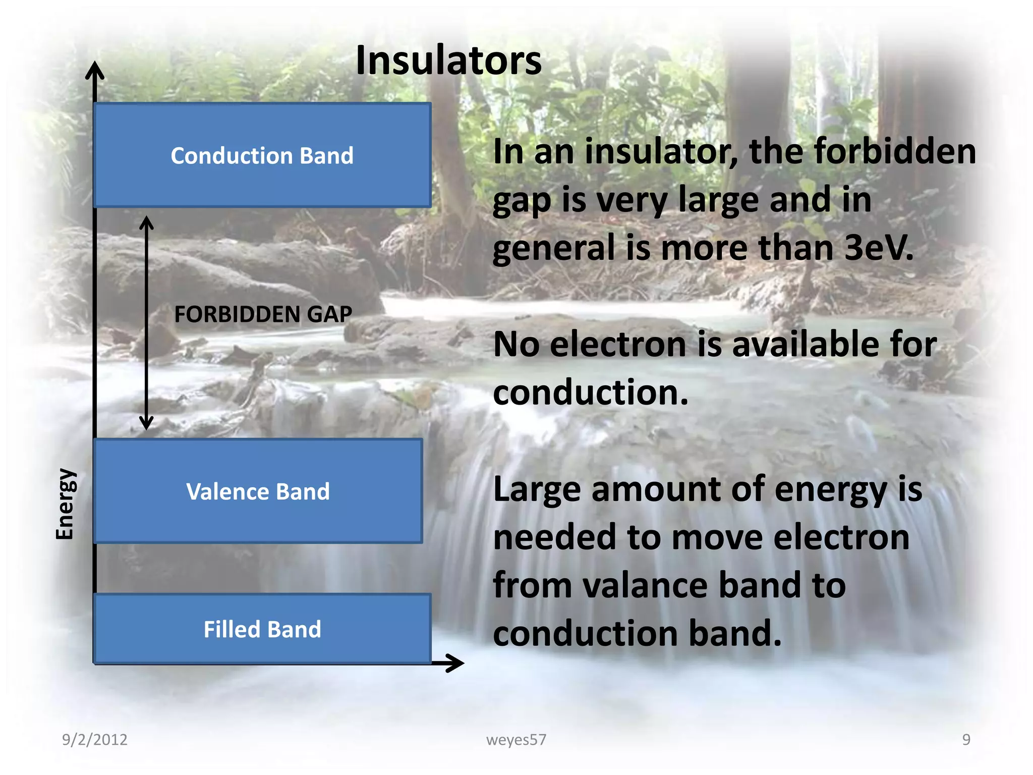
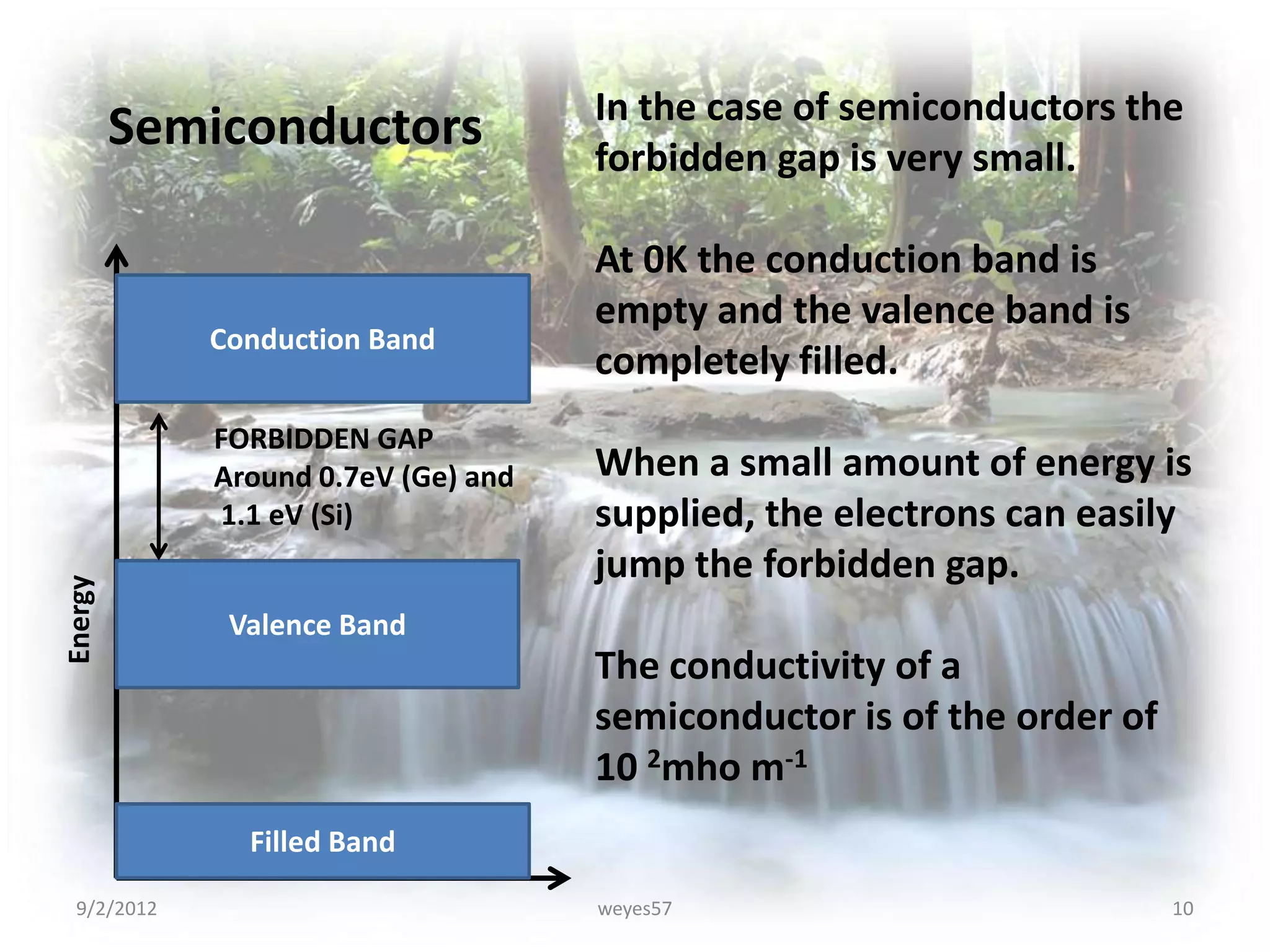
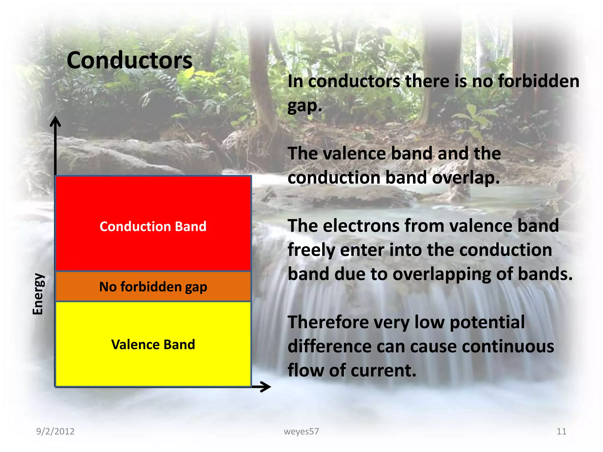
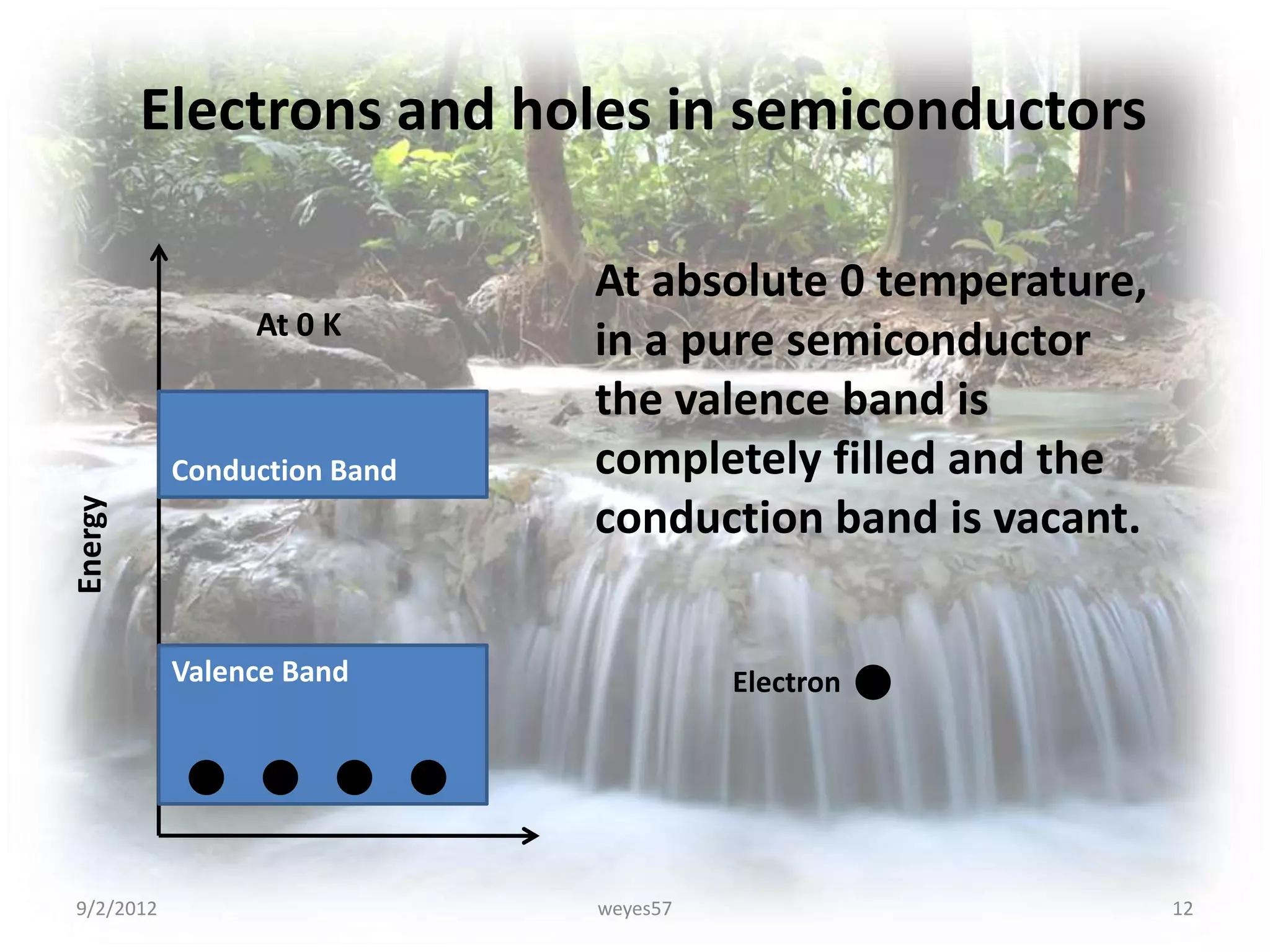
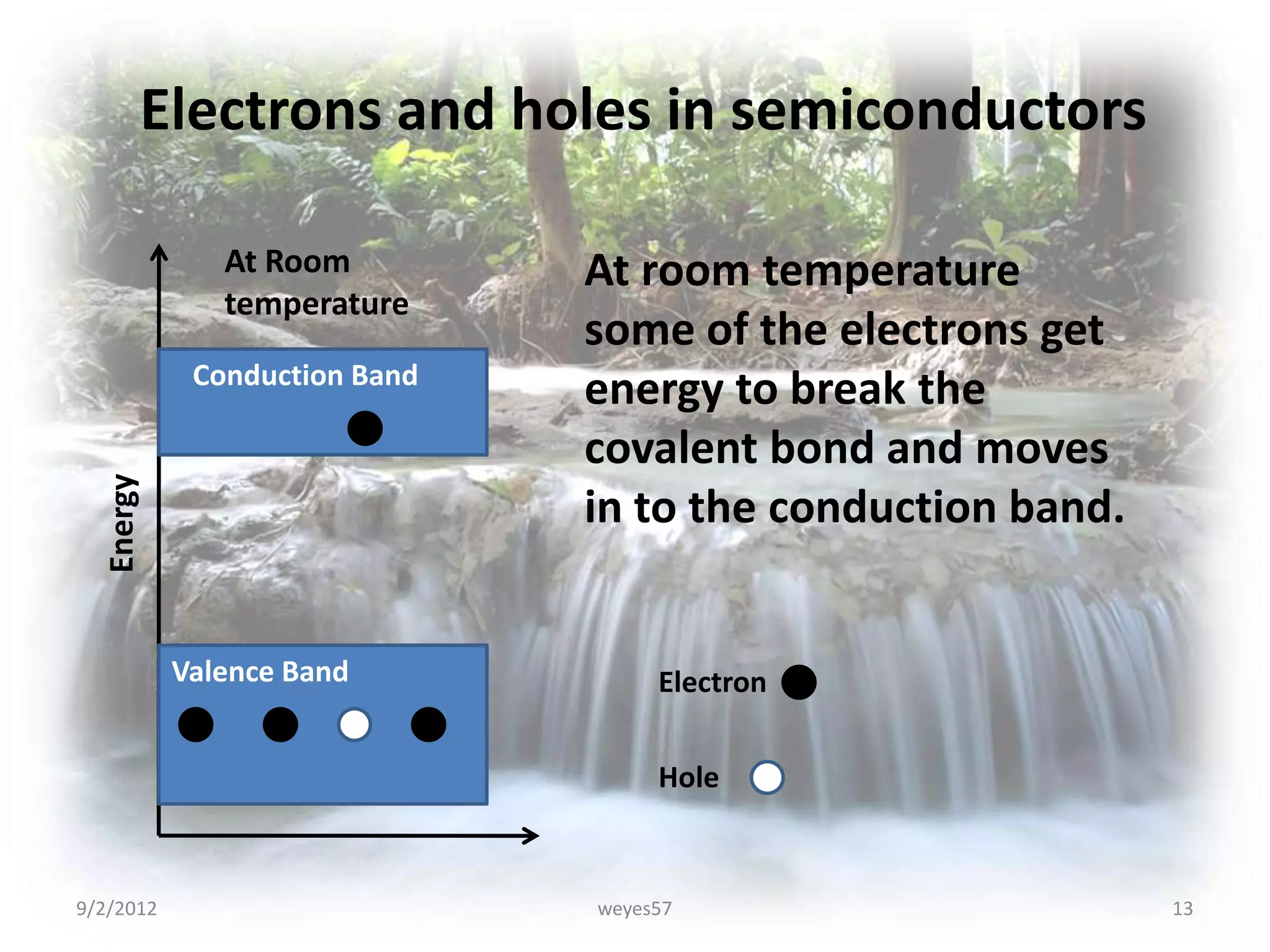
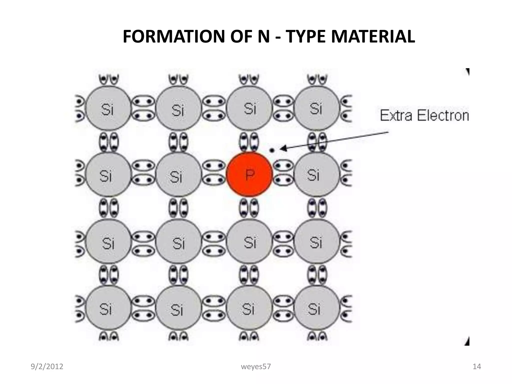
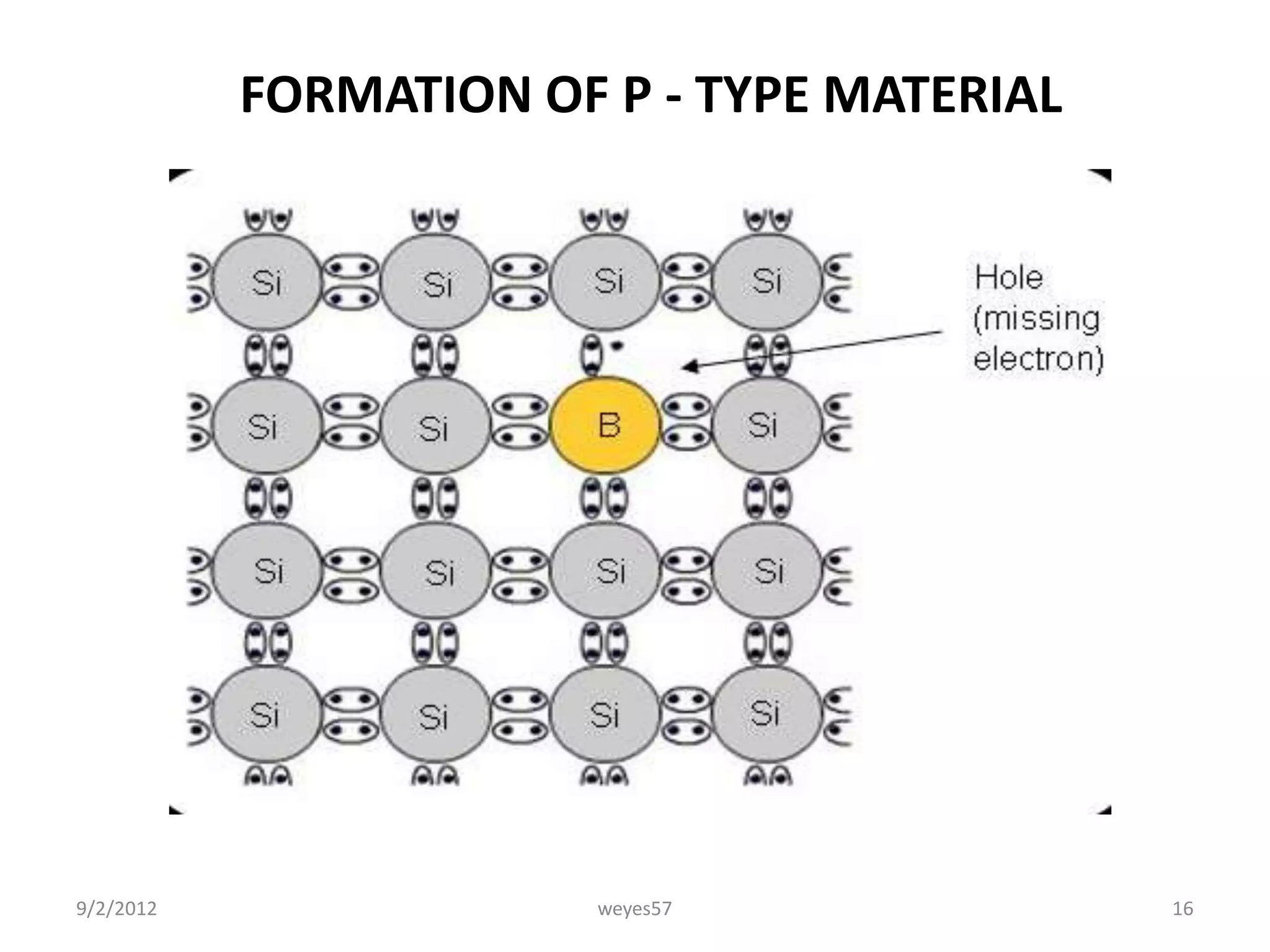


The document discusses semiconductors and their properties. It explains that semiconductors have resistivity between conductors and insulators. Their energy bands consist of a conduction band, valence band, and a small forbidden gap of around 0.7-1.1 eV. This allows electrons to move between bands with small amounts of energy. The document also describes intrinsic and extrinsic semiconductors, and how doping with elements from group 3 or 5 creates an excess or deficiency of electrons, resulting in n-type or p-type materials respectively.


