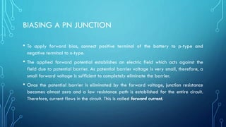
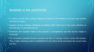
The document summarizes key concepts about semiconductors and pn junctions. It discusses how semiconductors have properties between conductors and insulators. Intrinsic semiconductors have few charge carriers, while extrinsic semiconductors are doped with impurities to increase charge carriers, making them n-type or p-type. A pn junction forms at the interface of a p-type and n-type semiconductor, creating a depletion region and potential barrier. Forward biasing reduces and reverse biasing increases the potential barrier.
Introduction to Semiconductor Devices.
In modern world no other technology permeates every nook and cranny of our existence as does electronics.
Application of electronics are : Televisions, radios, stereo equipment, computers, scanners, electronic control systems (in cars for example) etc.
This ppt is about semiconductor diodes.You can get every basic information about PN junction diode and its working and some more information about the semiconductors.
Fundamentals of learn how to Semiconductors can easily be mani pulated to become conducting or insulating materials and can change their conductive properties
MPLS VPN is a family of methods for using multiprotocol label switching (MPLS) to create virtual private networks (VPNs). MPLS VPN is a flexible method to transport and route several types of network traffic using an MPLS backbone.
The field of artificial intelligence (AI) has witnessed tremendous growth in recent years with the advent of Deep Neural Networks (DNNs) that surpass humans in a variety of cognitive tasks.
Cosmetic shop management system project report.pdfKamal Acharya
Buying new cosmetic products is difficult. It can even be scary for those who have sensitive skin and are prone to skin trouble. The information needed to alleviate this problem is on the back of each product, but it's thought to interpret those ingredient lists unless you have a background in chemistry.
Instead of buying and hoping for the best, we can use data science to help us predict which products may be good fits for us. It includes various function programs to do the above mentioned tasks.
Data file handling has been effectively used in the program.
The automated cosmetic shop management system should deal with the automation of general workflow and administration process of the shop. The main processes of the system focus on customer's request where the system is able to search the most appropriate products and deliver it to the customers. It should help the employees to quickly identify the list of cosmetic product that have reached the minimum quantity and also keep a track of expired date for each cosmetic product. It should help the employees to find the rack number in which the product is placed.It is also Faster and more efficient way.
NO1 Uk best vashikaran specialist in delhi vashikaran baba near me online vas...Amil Baba Dawood bangali
Contact with Dawood Bhai Just call on +92322-6382012 and we'll help you. We'll solve all your problems within 12 to 24 hours and with 101% guarantee and with astrology systematic. If you want to take any personal or professional advice then also you can call us on +92322-6382012 , ONLINE LOVE PROBLEM & Other all types of Daily Life Problem's.Then CALL or WHATSAPP us on +92322-6382012 and Get all these problems solutions here by Amil Baba DAWOOD BANGALI
#vashikaranspecialist #astrologer #palmistry #amliyaat #taweez #manpasandshadi #horoscope #spiritual #lovelife #lovespell #marriagespell#aamilbabainpakistan #amilbabainkarachi #powerfullblackmagicspell #kalajadumantarspecialist #realamilbaba #AmilbabainPakistan #astrologerincanada #astrologerindubai #lovespellsmaster #kalajaduspecialist #lovespellsthatwork #aamilbabainlahore#blackmagicformarriage #aamilbaba #kalajadu #kalailam #taweez #wazifaexpert #jadumantar #vashikaranspecialist #astrologer #palmistry #amliyaat #taweez #manpasandshadi #horoscope #spiritual #lovelife #lovespell #marriagespell#aamilbabainpakistan #amilbabainkarachi #powerfullblackmagicspell #kalajadumantarspecialist #realamilbaba #AmilbabainPakistan #astrologerincanada #astrologerindubai #lovespellsmaster #kalajaduspecialist #lovespellsthatwork #aamilbabainlahore #blackmagicforlove #blackmagicformarriage #aamilbaba #kalajadu #kalailam #taweez #wazifaexpert #jadumantar #vashikaranspecialist #astrologer #palmistry #amliyaat #taweez #manpasandshadi #horoscope #spiritual #lovelife #lovespell #marriagespell#aamilbabainpakistan #amilbabainkarachi #powerfullblackmagicspell #kalajadumantarspecialist #realamilbaba #AmilbabainPakistan #astrologerincanada #astrologerindubai #lovespellsmaster #kalajaduspecialist #lovespellsthatwork #aamilbabainlahore #Amilbabainuk #amilbabainspain #amilbabaindubai #Amilbabainnorway #amilbabainkrachi #amilbabainlahore #amilbabaingujranwalan #amilbabainislamabad
Overview of the fundamental roles in Hydropower generation and the components involved in wider Electrical Engineering.
This paper presents the design and construction of hydroelectric dams from the hydrologist’s survey of the valley before construction, all aspects and involved disciplines, fluid dynamics, structural engineering, generation and mains frequency regulation to the very transmission of power through the network in the United Kingdom.
Author: Robbie Edward Sayers
Collaborators and co editors: Charlie Sims and Connor Healey.
(C) 2024 Robbie E. Sayers
Water scarcity is the lack of fresh water resources to meet the standard water demand. There are two type of water scarcity. One is physical. The other is economic water scarcity.
Automobile Management System Project Report.pdfKamal Acharya
The proposed project is developed to manage the automobile in the automobile dealer company. The main module in this project is login, automobile management, customer management, sales, complaints and reports. The first module is the login. The automobile showroom owner should login to the project for usage. The username and password are verified and if it is correct, next form opens. If the username and password are not correct, it shows the error message.
When a customer search for a automobile, if the automobile is available, they will be taken to a page that shows the details of the automobile including automobile name, automobile ID, quantity, price etc. “Automobile Management System” is useful for maintaining automobiles, customers effectively and hence helps for establishing good relation between customer and automobile organization. It contains various customized modules for effectively maintaining automobiles and stock information accurately and safely.
When the automobile is sold to the customer, stock will be reduced automatically. When a new purchase is made, stock will be increased automatically. While selecting automobiles for sale, the proposed software will automatically check for total number of available stock of that particular item, if the total stock of that particular item is less than 5, software will notify the user to purchase the particular item.
Also when the user tries to sale items which are not in stock, the system will prompt the user that the stock is not enough. Customers of this system can search for a automobile; can purchase a automobile easily by selecting fast. On the other hand the stock of automobiles can be maintained perfectly by the automobile shop manager overcoming the drawbacks of existing system.
Courier management system project report.pdfKamal Acharya
It is now-a-days very important for the people to send or receive articles like imported furniture, electronic items, gifts, business goods and the like. People depend vastly on different transport systems which mostly use the manual way of receiving and delivering the articles. There is no way to track the articles till they are received and there is no way to let the customer know what happened in transit, once he booked some articles. In such a situation, we need a system which completely computerizes the cargo activities including time to time tracking of the articles sent. This need is fulfilled by Courier Management System software which is online software for the cargo management people that enables them to receive the goods from a source and send them to a required destination and track their status from time to time.
Industrial Training at Shahjalal Fertilizer Company Limited (SFCL)MdTanvirMahtab2
This presentation is about the working procedure of Shahjalal Fertilizer Company Limited (SFCL). A Govt. owned Company of Bangladesh Chemical Industries Corporation under Ministry of Industries.
Explore the innovative world of trenchless pipe repair with our comprehensive guide, "The Benefits and Techniques of Trenchless Pipe Repair." This document delves into the modern methods of repairing underground pipes without the need for extensive excavation, highlighting the numerous advantages and the latest techniques used in the industry.
Learn about the cost savings, reduced environmental impact, and minimal disruption associated with trenchless technology. Discover detailed explanations of popular techniques such as pipe bursting, cured-in-place pipe (CIPP) lining, and directional drilling. Understand how these methods can be applied to various types of infrastructure, from residential plumbing to large-scale municipal systems.
Ideal for homeowners, contractors, engineers, and anyone interested in modern plumbing solutions, this guide provides valuable insights into why trenchless pipe repair is becoming the preferred choice for pipe rehabilitation. Stay informed about the latest advancements and best practices in the field.
Forklift Classes Overview by Intella PartsIntella Parts
Discover the different forklift classes and their specific applications. Learn how to choose the right forklift for your needs to ensure safety, efficiency, and compliance in your operations.
For more technical information, visit our website https://intellaparts.com
Hybrid optimization of pumped hydro system and solar- Engr. Abdul-Azeez.pdffxintegritypublishin
Advancements in technology unveil a myriad of electrical and electronic breakthroughs geared towards efficiently harnessing limited resources to meet human energy demands. The optimization of hybrid solar PV panels and pumped hydro energy supply systems plays a pivotal role in utilizing natural resources effectively. This initiative not only benefits humanity but also fosters environmental sustainability. The study investigated the design optimization of these hybrid systems, focusing on understanding solar radiation patterns, identifying geographical influences on solar radiation, formulating a mathematical model for system optimization, and determining the optimal configuration of PV panels and pumped hydro storage. Through a comparative analysis approach and eight weeks of data collection, the study addressed key research questions related to solar radiation patterns and optimal system design. The findings highlighted regions with heightened solar radiation levels, showcasing substantial potential for power generation and emphasizing the system's efficiency. Optimizing system design significantly boosted power generation, promoted renewable energy utilization, and enhanced energy storage capacity. The study underscored the benefits of optimizing hybrid solar PV panels and pumped hydro energy supply systems for sustainable energy usage. Optimizing the design of solar PV panels and pumped hydro energy supply systems as examined across diverse climatic conditions in a developing country, not only enhances power generation but also improves the integration of renewable energy sources and boosts energy storage capacities, particularly beneficial for less economically prosperous regions. Additionally, the study provides valuable insights for advancing energy research in economically viable areas. Recommendations included conducting site-specific assessments, utilizing advanced modeling tools, implementing regular maintenance protocols, and enhancing communication among system components.
Saudi Arabia stands as a titan in the global energy landscape, renowned for its abundant oil and gas resources. It's the largest exporter of petroleum and holds some of the world's most significant reserves. Let's delve into the top 10 oil and gas projects shaping Saudi Arabia's energy future in 2024.
2. INTRODUCTION
• Certain substances like germanium, silicon, carbon etc. are neither good
conductors nor insulators.
• In other words, the resistivity of these materials lies inbetween conductors and
insulators.
• Such substances are classified as semiconductors.
• Semiconductors have some useful properties and are being extensively used in
electronic circuits.
3. SEMICONDUCTOR
• A semiconductor is a substance which has resistivity (10−4 to 0.5 Ωm) inbetween
conductors and insulators e.g. germanium, silicon, selenium, carbon etc.
• Properties of Semiconductors
i. The resistivity of a semiconductor is less than an insulator but more than a conductor.
ii. Semiconductors have negative temperature co-efficient of resistance i.e. the
resistance of a semiconductor decreases with the increase in temperature and vice-
versa.
iii. When a suitable metallic impurity is added to a semiconductor, its current conducting
properties change appreciably.
4. BONDS IN SEMICONDUCTORS
• The atoms of every element are held together by the bonding action of valence
electrons.
• In semiconductors, bonds are formed by sharing of valence electrons. Such bonds are
called co-valent bonds.
i. Co-valent bonds are formed by sharing of valence electrons.
ii. In the formation of co-valent bond, each valence electron of an atom forms direct
bond with the valence electron of an adjacent atom.
iii. Valence electrons are associated with particular atoms. For this reason, valence
electrons in a semiconductor are not free.
5. COMMONLY USED SEMICONDUCTORS
• There are many semiconductors available, but very few of them have a practical
application in electronics.
• The two most frequently used materials are germanium (Ge) and silicon (Si).
• It is because the energy required to break their co-valent bonds is very small; being about
0.7 eV for germanium and about 1.1 eV for silicon.
• Germanium has become the model substance among the semiconductors; the main reason
being that it can be purified relatively well and crystallised easily.
• The silicon compounds are chemically reduced to silicon which is 100% pure for use as a
semiconductor.
6. EFFECT OF TEMPERATURE ON SEMICONDUCTORS
• The electrical conductivity of a semiconductor changes appreciably with temperature
variations.
• At absolute zero temperature, all the electrons are tightly held by the semiconductor
atoms. At this temperature, the co-valent bonds are very strong and there are no free
electrons. Therefore, the semiconductor crystal behaves as a perfect insulator.
• When the temperature is raised, some of the covalent bonds in the semiconductor break
due to the thermal energy supplied. The breaking of bonds sets those electrons free which
are engaged in the formation of these bonds.The result is that a few free electrons exist in
the semiconductor. These free electrons can constitute a tiny electric current.
This shows that the resistance of a semiconductor decreases with the rise in temperature
7. INTRINSIC SEMICONDUCTOR
• A semiconductor in an extremely pure form is known as an intrinsic semiconductor.
• In an intrinsic semiconductor, even at room temperature, hole-electron pairs are created.
When electric field is applied across an intrinsic semiconductor, the current conduction
takes place by two processes, namely ; by free electrons and holes. The free electrons
are produced due to the breaking up of some covalent bonds by thermal energy. At the
same time, holes are created in the covalent bonds. Under the influence of electric field,
conduction through the semiconductor is by both free electrons and holes. Therefore, the
total current inside the semiconductor is the sum of currents due to free electrons and
holes.
8. EXTRINSIC SEMICONDUCTOR
• The intrinsic semiconductor has little current conduction capability at room
temperature.
• To be useful in electronic devices, the pure semiconductor must be altered so
as to significantly increase its conducting properties. This is achieved by
adding a small amount of suitable impurity to a semiconductor. It is then called
impurity or extrinsic semiconductor.
• The process of adding impurities to asemiconductor is known as doping.
9. EXTRINSIC SEMICONDUCTOR
• The purpose of adding impurity is to increase either the number of free electrons or holes
in the semiconductor crystal.
• If a pentavalent impurity (having 5 valence electrons) is added to the semiconductor, a
large number of free electrons are produced in the semiconductor.
• On the other hand, addition of trivalent impurity (having 3 valence electrons) creates a
large number of holes in the semiconductor crystal.
• Depending upon the type of impurity added, extrinsic semiconductors are classified into:
• (i) n-type semiconductor (ii) p-type semiconductor
10. N-TYPE SEMICONDUCTOR
• When a small amount of pentavalent impurity is added to a pure semiconductor, it is
known as n-type semiconductor.
• The addition of pentavalent impurity provides a large number of free electrons in the
semiconductor crystal.
• Typical examples of pentavalent impurities are arsenic and antimony.
• Such impurities which produce n-type semiconductor are known as donor impurities
because they donate or provide free electrons to the semiconductor crystal.
11. N-TYPE SEMICONDUCTOR
• When a small amount of pentavalent impurity like arsenic is added to a semiconductor
like germanium crystal, a large number of free electrons become available in the crystal.
• Arsenic is pentavalent i.e. its atom has five valence electrons. An arsenic atom fits in the
germanium crystal in such a way that its four valence electrons form covalent bonds with
four germanium atoms. The fifth valence electron of arsenic atom finds no place in co-
valent bonds and is thus free
• Therefore, for each arsenic atom added, one free electron will be available in the
germanium crystal. Thus the addition of pentavalent impurity produces a number of
conduction band electrons i.e., free electrons.
12. P-TYPE SEMICONDUCTOR
• When a small amount of trivalent impurity is added to a pure semiconductor,
it is called p-type semiconductor.
• The addition of trivalent impurity provides a large number of holes in the
semiconductor.
• Typical examples of trivalent impurities are gallium and indium.
• Such impurities which produce p-type semiconductor are known as acceptor
impurities because the holes created can accept the electrons.
13. P-TYPE SEMICONDUCTOR
• When a small amount of trivalent impurity like gallium is added to germanium crystal, there
exists a large number of holes in the crystal.
• Gallium is trivalent i.e. its atom has three valence electrons.
• Each atom of gallium fits into the germanium crystal but now only three co-valent bonds can
be formed. It is because three valence electrons of gallium atom can form only three single
co-valent bonds with three germanium atoms.
• In the fourth co-valent bond, only germanium atom contributes one valence electron while
gallium has no valence electron to contribute.
• This missing electron is called a hole. Therefore, for each gallium atom added, one hole is
created.
14. CHARGE ON N-TYPE AND P-TYPE SEMICONDUCTORS
• In n-type semiconductor, current conduction is due to excess of electrons whereas in a p-type
semiconductor, conduction is by holes.
• The n-type semiconductor has excess of electrons but these extra electrons were supplied by the
atoms of donor impurity and each atom of donor impurity is electrically neutral.
• When the impurity atom is added, the term “excess electrons” refers to an excess with regard to the
number of electrons needed to fill the co-valent bonds in the semiconductor crystal.
• The extra electrons are free electrons and increase the conductivity of the semiconductor. The
situation with regard to p-type semiconductor is also similar.
It follows, therefore, that n-type as well as p-type semiconductor is electrically neutral.
15. PN JUNCTION
• When a p-type semiconductor is suitably joined to n-type semiconductor, the contact
surface is called pn junction.
• Most semiconductor devices contain one or more pn junctions. The pn junction is of great
importance because it is in effect, the control element for semiconductor devices.
• At the instant of pn-junction formation, the free electrons near the junction in the n region
begin to diffuse across the junction into the p region where they combine with holes near
the junction.
• This creates a layer of positive charges (pentavalent ions) near the junction.
16. PN JUNCTION
• As the electrons move across the junction, the p region loses holes as the electrons and
holes combine.
• The result is that there is a layer of negative charges (trivalent ions) near the junction.
• These two layers of positive and negative charges form the depletion region (or
depletion layer).
• The term depletion is due to the fact that near the junction, the region is depleted of
charge carries due to diffusion across the junction.
• It may be noted that depletion layer is formed very quickly and is very thin compared
to the n region and the p region.
17. BIASING A PN JUNCTION
In electronics, the term bias refers to the use of d.c. voltage to establish certain operating
conditions for an electronic device. In relation to a pn junction, there are following two bias
conditions:
1. When external d.c. voltage applied to the junction is in such a direction that it cancels
the potential barrier, thus permitting current flow, it is called forward biasing.
2. When the external d.c. voltage applied to the junction is in such a direction that
potential barrier is increased, and no current flows across the circuit, it is called reverse
biasing.
18. BIASING A PN JUNCTION
• To apply forward bias, connect positive terminal of the battery to p-type and
negative terminal to n-type.
• The applied forward potential establishes an electric field which acts against the
field due to potential barrier. As potential barrier voltage is very small, therefore, a
small forward voltage is sufficient to completely eliminate the barrier.
• Once the potential barrier is eliminated by the forward voltage, junction resistance
becomes almost zero and a low resistance path is established for the entire circuit.
Therefore, current flows in the circuit. This is called forward current.
19. BIASING A PN JUNCTION
• To apply reverse bias, connect negative terminal of the battery to p-type and positive
terminal to n-type.
• Applied reverse voltage establishes an electric field which acts in the same direction as
the field due to potential barrier.
• Therefore, the resultant field at the junction is strengthened and the barrier height is
increased.
• The increased potential barrier prevents the flow of charge carriers across the junction.
Thus, a high resistance path is established for the entire circuit and hence the current does
not flow.