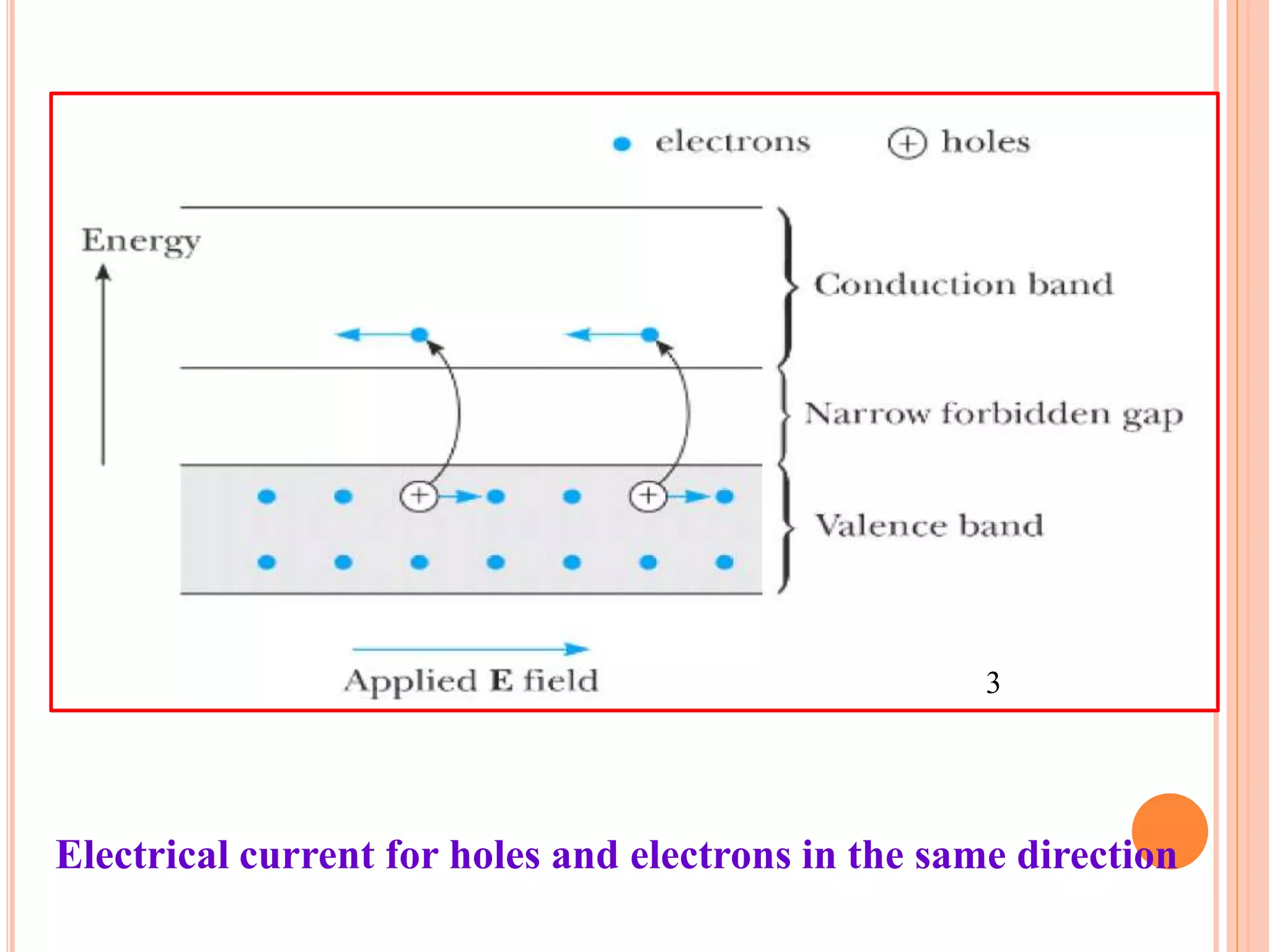
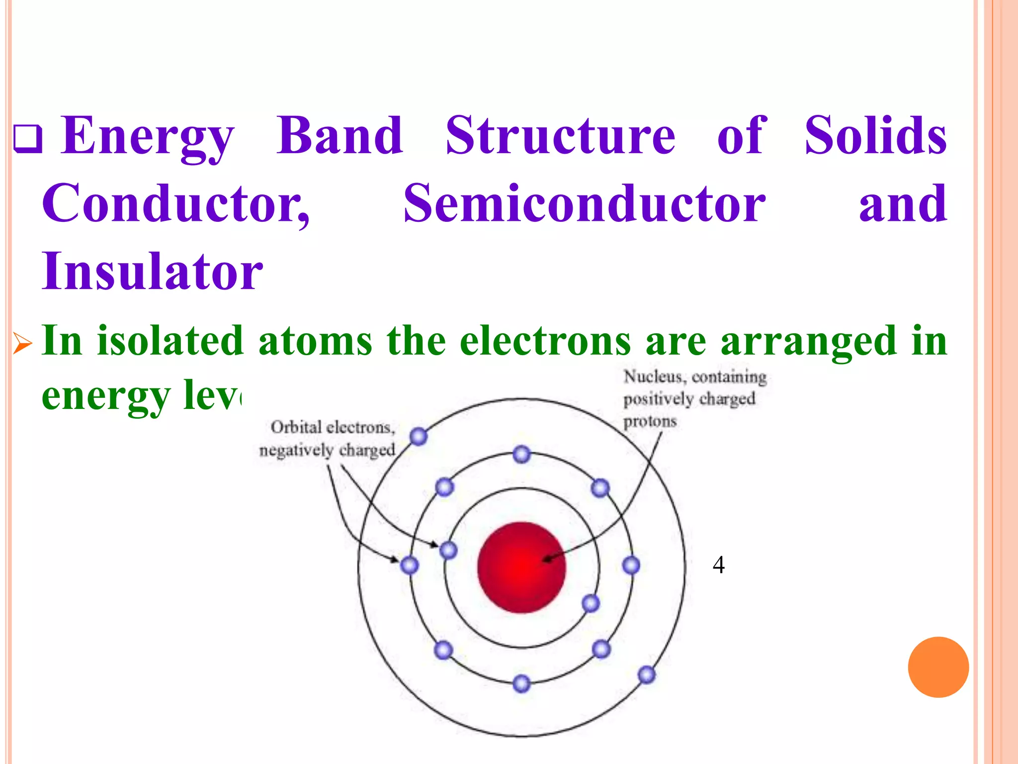
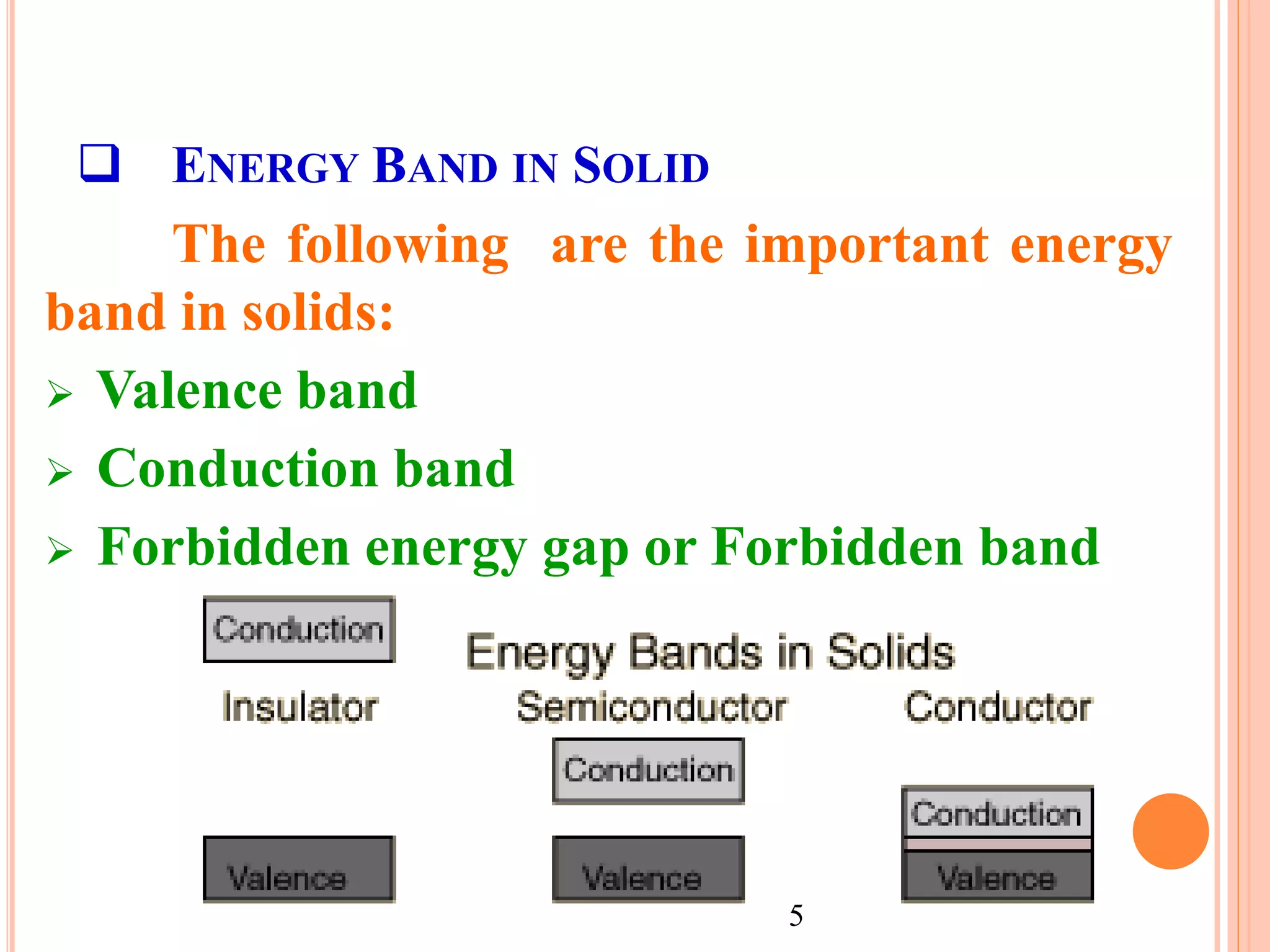
BAND THEORY OF
SOLID
Course: B.Tech
Subject: Engineering Physics
Unit: I
Chapter: 2
 OBJECTIVES
• Effective Mass of electron
• Concept of Holes
• Energy Band Structure of Solids:
 Conductors, Insulators and Semiconductors
• Semiconductors
 Intrinsic and Extrinsic Semiconductors
• Type of diodes
 Simple Diode
 Zener Diode
 EFFECTIVE MASS OF ELECTRON
 An electron moving in the solid under the
influence of the crystal potential is subjected to
an electric field.
 We expect an external field to accelerate the
electron, increasing E and k and change the
electron’s state.
1
dt
dx
dx
dV
e
dt
dV
e
dt
d
eV




and
dk
d
gv


1

gv
dx
dV
e
dt
dk
dk
d


dx
dV
ek
dt
d
gv
dx
dV
e
dt
dk
gv




eEk
dt
d

dt
dk
dk
d
dk
d
dk
d
dt
d
dt
dv
a
g















11




















k
dt
d
dk
d
dt
dk
dk
d

 2
2
22
2
11 
eE = F
e
1
m
1
2
2
2e
1










dk
d
m


Effective Mass Revisited
 This relates the curvature of the band to the “effective
mass.”
 One can show that a free electron “band” gives an effective
mass equal to the rest mass of an electron.
 Electrons in a crystal are accelerated in response to an
external force just as though they were free electrons with
effective mass me.
 Usually , me < m0.(m0=9.1 x 10⁻³¹kg)
 CONCEPT OF HOLES
 Consider a semiconductor with a small
number of electrons excited from the valence
band into the conduction band.
 If an electric field is applied,
• the conduction band electrons will
participate in the electrical current
• the valence band electrons can “move
into” the empty states, and thus can also
contribute to the current.
2
 CONCEPT OF HOLES
 If we describe such changes via “movement” of
the “empty” states – the picture will be
significantly simplified. This “empty space” is
called a Hole.
 “Deficiency” of negative charge can be treated
as a positive charge.
 Holes act as charge carriers in the sense that
electrons from nearby sites can “move” into the
hole.
 Holes are usually heavier than electrons since
they depict collective behavior of many
electrons.
Electrical current for holes and electrons in the same direction
3
To understand hole motion, one requires
another view of the holes, which represent
them as electrons with negative effective mass
m*.
For example the movement of the hole think
of a row of chairs occupied by people with one
chair empty, and to move all people rise all
together and move in one direction, so the
empty spot moves in the same direction
 Energy Band Structure of Solids
Conductor, Semiconductor and
Insulator
 In isolated atoms the electrons are arranged in
energy levels.
4
 ENERGY BAND IN SOLID
The following are the important energy
band in solids:
 Valence band
 Conduction band
 Forbidden energy gap or Forbidden band
5
Valance band
The band of energy occupied by the valance
electrons is called valence band. The electrons in
the outermost orbit of an atom are known as
valance electrons. This band may be completely or
partial filled.
Electron can be move from one valance band
to the conduction band by the application of
external energy.
 Conduction band
The band of energy occupied by the
conduction electrons is called conduction band.
This is the uppermost band and all electrons in the
conduction band are free electrons.
The conduction band is empty for insulator
and partially filled for conductors.
 Forbidden Energy Gap or Forbidden band
The gap between the valance band and
conduction band on energy level diagram known as
forbidden band or energy gap.
Electron are never found in the gap. Electrons
may jump from back and forth from the bottom of
valance band to the top of the conduction band. But
they never come to rest in the forbidden band.
 According to the classical free electron
theory, materials are classified in to three
types:
 Conductors
 Semiconductors
 Insulators
Conductors
There is no forbidden gap and the conduction
band and valence band are overlapping each other
between and hence electrons are free to move about.
Examples are Ag, Cu, Fe, Al, Pb ….
 Conductor are highly electrical conductivity.
 So, in general electrical resistivity of conductor is
very low and it is of the order of 10-6 Ω cm.
 Due to the absence of the forbidden gap, there is no
structure for holes.
 The total current in conductor is simply a flow of
electrons.
 For conductors, the energy gap is of the order of
0.01 eV.
Semiconductors
Semiconductors are materials whose electrical
resistivity lies between insulator and conductor.
Examples are silicon (Si), germanium (Ge) ….
 The resistivity of semiconductors lie between 10-4 Ω
cm to 103 Ω cm at room temperature.
 At low temperature, the valence band is all most full
and conduction band is almost empty. The forbidden
gap is very small equal to 1 eV.
 Semiconductor behaves like an insulator at low
temperature. The most commonly used
semiconductor is silicon and its band gap is 1.21 eV
and germanium band gap is 0.785 eV.
When a conductor is heated its
resistance increases; The atoms vibrate more
and the electrons find it more difficult to move
through the conductor but, in a
semiconductor the resistance decreases with
an increase in temperature. Electrons can be
excited up to the conduction band and
Conductivity increases.
6
Insulators
In insulator, the valence band is full but the
conduction band is totally empty. So, free electrons
from conduction band is not available.
 In insulator the energy gap between the valence and
conduction band is very large and its approximately
equal to 5 eV or more.
 Hence electrons cannot jump from valence band to
the conduction band. So, a very high energy is
required to push the electrons to the conduction
band.
 The electrical conductivity is extremely small.
 The resistivity of insulator lie between 103 to 1017
Ωm, at the room temperature
 Examples are plastics, paper …..
 TYPES OF SEMICONDUCTORS
Semiconductors
Intrinsic Semiconductor Extrinsic Semiconductor
p - type n - type
 INTRINSIC SEMICONDUCTOR
 The intrinsic semiconductor are pure semiconductor
materials.
 These semiconductors posses poor conductivity.
 The elemental and compound semiconductor can be
intrinsic type.
 The energy gap in semiconductor is very small.
 So even at the room temperature, some of electrons from
valance band can jump to the conduction band by
thermal energy.
 The jump of electron in conduction band adds one
conduction electron in conduction band and creates a
hole in the valence band. The process is called as
“generation of an electron–hole pair”.
 In pure semiconductor the no. of electrons in conduction
band and holes in holes in valence bands are equal.
 EXTRINSIC SEMICONDUCTOR
 Extrinsic semiconductor is an impure semiconductor
formed from an intrinsic semiconductor by adding a
small quantity of impurity atoms called dopants.
 The process of adding impurities to the
semiconductor crystal is known as doping.
 This added impurity is very small of the order of one
atom per million atoms of pure semiconductor.
 Depending upon the type of impurity added the
extrinsic semiconductors are classified as:
(1) p – type semiconductor
(2) n – type semiconductor
The application of band theory to n-type and
p-type semiconductors shows that extra levels have been
added by the impurities.
In n-type material there are electron energy levels
near the top of the band gap so that they can be easily
excited into the conduction band.
In p-type material, extra holes in the band gap allow
excitation of valence band electrons, leaving mobile holes in
the valence band.
7
P – TYPE SEMICONDUCTOR
The addition of trivalent impurities such as
boron, aluminum or gallium to an intrinsic
semiconductor creates deficiencies of valence
electrons,called "holes". It is typical to use
B2H6 diborane gas to diffuse boron into the silicon
material.
8
N – TYPE SEMICONDUCTOR
The addition of pentavalent impurities such as
antimony, arsenic or phosphorous contributes free
electrons, greatly increasing the conductivity of the
intrinsic semiconductor. Phosphorous may be added
by diffusion of phosphine gas (PH3).
9
 SIMPLE DIODE (P N- JUNCTION
DIODE)
 The two terminals are called Anode and Cathode.
 At the instant the two materials are “joined”, electrons
and holes near the junction cross over and combine with
each other.
 Holes cross from P-side to N-side and Free electrons
cross from N-side to P-side.
 At P-side of junction, negative ions are formed.
 At N-side of junction, positive ions are formed.
10
 Depletion region is the region having no free carriers.
 Further movement of electrons and holes across the junction
stops due to formation of depletion region.
11
 Depletion region acts as barrier opposing further
diffusion of charge carriers. So diffusion stops within
no time.
 Current through the diode under no-bias condition is
zero.
REVERSE BIAS
 Positive of battery connected to n-type material (cathode).
 Negative of battery connected to p-type material (anode).
12
REVERSE BIAS…..
 Free electrons in n-region are drawn towards
positive of battery, Holes in p-region are drawn
towards negative of battery.
 Depletion region widens, barrier increases for the
flow of majority carriers.
 Majority charge carrier flow reduces to zero.
 Minority charge carriers generated thermally can
cross the junction – results in a current called
“reverse saturation current” Is , Is is in micro or
nano amperes or less. Is does not increase
“significantly” with increase in the reverse bias
voltage
FORWARD BIAS
 Positive of battery connected to p-type (anode)
 Negative of battery connected to n-type (cathode)
13
FORWARD BIAS…
 Electrons in n-type are forced to recombine with
positive ions near the boundary, similarly holes in
p-type are forced to recombine with negative ions.
 Depletion region width reduces.
 An electron in n-region “sees” a reduced barrier at
the junction and strong attraction for positive
potential.
 As forward bias is increased, depletion region
narrows down and finally disappears – leads to
exponential rise in current.
 Forward current is measured in milli amperes
14
 ZENER DIODE
A diode which is heavily doped and which
operates in the reverse breakdown region with a
sharp breakdown voltage is called a Zener diode.
This is similar to the normal diode except
that the line (bar) representing the cathode is
bent at both side ends like the letter Z for Zener
diode.
15
In simple diode the doping is light; as a
result, the breakdown voltage is high and not
sharp. But if doping is made heavy, then the
depletion layers becomes very narrow and even
the breakdown voltage gets reduced to a sharp
value.
 Working Principle
The reverse breakdown of a Zener diode
may occur either due to Zener effect or
avalanche effect. But the Zener diode is
primarily depends on Zener effect for its
working.
 When the electrical field across the
junction is high due to the applied voltage, the
Zener breakdown occurs because of breaking
of covalent bonds and produces a large number
of electrons and holes which constitute a steep
rise in the reverse saturation current (Zener
current IZ). This effect is called as Zener effect.
 Zener current IZ is independent of the
applied voltage and depends only on the
external resistance.
I-V CHARACTERISTIC OF A ZENER
DIODE
The forward characteristic is simply that
of an ordinary forward biased junction diode.
Under the reverse bias condition, the
breakdown of a junction occurs.
Its depends upon amount of doping. It can
be seen from above figure as the reverse voltage
is increased the reverse current remains
negligibly small up to the knee point (K) of the
curve.
 At point K, the effect of breakdown
process beings. The voltage corresponding to
the point K in figure is called the Zener
breakdown voltage or simply Zener voltage
(VZ), which is very sharp compared to a
simple p-n junction diode. Beyond this voltage
the reverse current (IZ) increases sharply to a
high value.
 The Zener diode is not immediately burnt
just because it has entered the breakdown
region.
 The Zener voltage VZ remains constant
even when Zener current I increases greatly.
The maximum value of current is denoted by
IZ max and the minimum current to sustain
breakdown is denoted by IZ min. By two points A
and B on the reverse VI characteristic, the Zener
resistance is given by the relation,
rz = ( Δ VZ / Δ IZ) -----(1)
16
 ZENER DIODE APPLICATIONS:
I. Zener diodes are used as a voltage
regulator.
II. They are used in shaping circuits as peak
limiters or clippers.
III. They are used as a fixed reference voltage
in transistor biasing and for comparison
purpose.
IV. They are used for meter protection against
damage from accidental application of
excessive voltage.
IMAGE REFERENCE LINKS
1. http://postimg.org/image/sl3tj8a71
2. http://web.utk.edu/~cnattras/Phys250Fall2012/modules/module%204/conduction_in_solids.htm
3. http://mystudyexpress.com/12%20th%20science%20cbse/physices/Electronic%20devices/unit%2
0image/1--band.gif
4. http://www.pixentral.com/pics/1JcifLv2C7L4gOi1EaDBtH6ZA51xkd.png
5. https://lh5.googleusercontent.com/-
16m5gmPuujM/VKZDTCWuH5I/AAAAAAAAAYE/c7hh5fUbsug/w475-h377-
no/New%2BPicture%2B%2825%29.png
6. http://s15.postimg.org/arf492z13/New_Picture_26.jpg?noCache=1420186429
7. http://hyperphysics.phy-astr.gsu.edu/hbase/solids/imgsol/bandop.gif
8. http://hyperphysics.phy-astr.gsu.edu/hbase/solids/imgsol/psem2.gif
9. http://hyperphysics.phy-astr.gsu.edu/hbase/solids/imgsol/nsem.gif
10. http://www.engineersgarage.com/sites/default/files/imagecache/Original/wysiwyg_imageupload/1
/Internal-structure-of-p-n-Diode.jpg
11. http://rsandas.com/images/Zener_Symbol.jpg
12. http://www.globalspec.com/ImageRepository/LearnMore/20131/diode58cd4e2f1b9114708851ac5
3e3d63e9c7.gif
13. https://encrypted-
tbn1.gstatic.com/images?q=tbn:ANd9GcSruAypsy5B4GX6xIrC2mzrjNqsA7bm8dNgnHeZ43Hz
C-8PSVBg
14. http://s3.postimg.org/wzdlbz75r/New_Picture_31.jpg?noCache=1420188304
15. http://s3.postimg.org/4rluv6sqn/New_Picture_32.jpg?noCache=1420188402
16. http://s13.postimg.org/hvt9cyghv/New_Picture_37.jpg?noCache=1420188443

B.tech sem i engineering physics u ii chapter 1-band theory of solid

  • 1.
    BAND THEORY OF SOLID Course:B.Tech Subject: Engineering Physics Unit: I Chapter: 2
  • 2.
     OBJECTIVES • EffectiveMass of electron • Concept of Holes • Energy Band Structure of Solids:  Conductors, Insulators and Semiconductors • Semiconductors  Intrinsic and Extrinsic Semiconductors • Type of diodes  Simple Diode  Zener Diode
  • 3.
     EFFECTIVE MASSOF ELECTRON  An electron moving in the solid under the influence of the crystal potential is subjected to an electric field.  We expect an external field to accelerate the electron, increasing E and k and change the electron’s state. 1
  • 4.
  • 5.
  • 6.
    1 2 2 2e 1           dk d m   Effective Mass Revisited This relates the curvature of the band to the “effective mass.”  One can show that a free electron “band” gives an effective mass equal to the rest mass of an electron.  Electrons in a crystal are accelerated in response to an external force just as though they were free electrons with effective mass me.  Usually , me < m0.(m0=9.1 x 10⁻³¹kg)
  • 7.
     CONCEPT OFHOLES  Consider a semiconductor with a small number of electrons excited from the valence band into the conduction band.  If an electric field is applied, • the conduction band electrons will participate in the electrical current • the valence band electrons can “move into” the empty states, and thus can also contribute to the current. 2
  • 8.
     CONCEPT OFHOLES  If we describe such changes via “movement” of the “empty” states – the picture will be significantly simplified. This “empty space” is called a Hole.  “Deficiency” of negative charge can be treated as a positive charge.  Holes act as charge carriers in the sense that electrons from nearby sites can “move” into the hole.  Holes are usually heavier than electrons since they depict collective behavior of many electrons.
  • 9.
    Electrical current forholes and electrons in the same direction 3
  • 10.
    To understand holemotion, one requires another view of the holes, which represent them as electrons with negative effective mass m*. For example the movement of the hole think of a row of chairs occupied by people with one chair empty, and to move all people rise all together and move in one direction, so the empty spot moves in the same direction
  • 11.
     Energy BandStructure of Solids Conductor, Semiconductor and Insulator  In isolated atoms the electrons are arranged in energy levels. 4
  • 12.
     ENERGY BANDIN SOLID The following are the important energy band in solids:  Valence band  Conduction band  Forbidden energy gap or Forbidden band 5
  • 13.
    Valance band The bandof energy occupied by the valance electrons is called valence band. The electrons in the outermost orbit of an atom are known as valance electrons. This band may be completely or partial filled. Electron can be move from one valance band to the conduction band by the application of external energy.
  • 14.
     Conduction band Theband of energy occupied by the conduction electrons is called conduction band. This is the uppermost band and all electrons in the conduction band are free electrons. The conduction band is empty for insulator and partially filled for conductors.
  • 15.
     Forbidden EnergyGap or Forbidden band The gap between the valance band and conduction band on energy level diagram known as forbidden band or energy gap. Electron are never found in the gap. Electrons may jump from back and forth from the bottom of valance band to the top of the conduction band. But they never come to rest in the forbidden band.
  • 16.
     According tothe classical free electron theory, materials are classified in to three types:  Conductors  Semiconductors  Insulators
  • 17.
    Conductors There is noforbidden gap and the conduction band and valence band are overlapping each other between and hence electrons are free to move about. Examples are Ag, Cu, Fe, Al, Pb ….  Conductor are highly electrical conductivity.  So, in general electrical resistivity of conductor is very low and it is of the order of 10-6 Ω cm.  Due to the absence of the forbidden gap, there is no structure for holes.  The total current in conductor is simply a flow of electrons.  For conductors, the energy gap is of the order of 0.01 eV.
  • 18.
    Semiconductors Semiconductors are materialswhose electrical resistivity lies between insulator and conductor. Examples are silicon (Si), germanium (Ge) ….  The resistivity of semiconductors lie between 10-4 Ω cm to 103 Ω cm at room temperature.  At low temperature, the valence band is all most full and conduction band is almost empty. The forbidden gap is very small equal to 1 eV.  Semiconductor behaves like an insulator at low temperature. The most commonly used semiconductor is silicon and its band gap is 1.21 eV and germanium band gap is 0.785 eV.
  • 19.
    When a conductoris heated its resistance increases; The atoms vibrate more and the electrons find it more difficult to move through the conductor but, in a semiconductor the resistance decreases with an increase in temperature. Electrons can be excited up to the conduction band and Conductivity increases. 6
  • 20.
    Insulators In insulator, thevalence band is full but the conduction band is totally empty. So, free electrons from conduction band is not available.  In insulator the energy gap between the valence and conduction band is very large and its approximately equal to 5 eV or more.  Hence electrons cannot jump from valence band to the conduction band. So, a very high energy is required to push the electrons to the conduction band.  The electrical conductivity is extremely small.  The resistivity of insulator lie between 103 to 1017 Ωm, at the room temperature  Examples are plastics, paper …..
  • 21.
     TYPES OFSEMICONDUCTORS Semiconductors Intrinsic Semiconductor Extrinsic Semiconductor p - type n - type
  • 22.
     INTRINSIC SEMICONDUCTOR The intrinsic semiconductor are pure semiconductor materials.  These semiconductors posses poor conductivity.  The elemental and compound semiconductor can be intrinsic type.  The energy gap in semiconductor is very small.  So even at the room temperature, some of electrons from valance band can jump to the conduction band by thermal energy.  The jump of electron in conduction band adds one conduction electron in conduction band and creates a hole in the valence band. The process is called as “generation of an electron–hole pair”.  In pure semiconductor the no. of electrons in conduction band and holes in holes in valence bands are equal.
  • 23.
     EXTRINSIC SEMICONDUCTOR Extrinsic semiconductor is an impure semiconductor formed from an intrinsic semiconductor by adding a small quantity of impurity atoms called dopants.  The process of adding impurities to the semiconductor crystal is known as doping.  This added impurity is very small of the order of one atom per million atoms of pure semiconductor.  Depending upon the type of impurity added the extrinsic semiconductors are classified as: (1) p – type semiconductor (2) n – type semiconductor
  • 24.
    The application ofband theory to n-type and p-type semiconductors shows that extra levels have been added by the impurities. In n-type material there are electron energy levels near the top of the band gap so that they can be easily excited into the conduction band. In p-type material, extra holes in the band gap allow excitation of valence band electrons, leaving mobile holes in the valence band. 7
  • 25.
    P – TYPESEMICONDUCTOR The addition of trivalent impurities such as boron, aluminum or gallium to an intrinsic semiconductor creates deficiencies of valence electrons,called "holes". It is typical to use B2H6 diborane gas to diffuse boron into the silicon material. 8
  • 26.
    N – TYPESEMICONDUCTOR The addition of pentavalent impurities such as antimony, arsenic or phosphorous contributes free electrons, greatly increasing the conductivity of the intrinsic semiconductor. Phosphorous may be added by diffusion of phosphine gas (PH3). 9
  • 27.
     SIMPLE DIODE(P N- JUNCTION DIODE)  The two terminals are called Anode and Cathode.  At the instant the two materials are “joined”, electrons and holes near the junction cross over and combine with each other.  Holes cross from P-side to N-side and Free electrons cross from N-side to P-side.  At P-side of junction, negative ions are formed.  At N-side of junction, positive ions are formed. 10
  • 28.
     Depletion regionis the region having no free carriers.  Further movement of electrons and holes across the junction stops due to formation of depletion region. 11
  • 29.
     Depletion regionacts as barrier opposing further diffusion of charge carriers. So diffusion stops within no time.  Current through the diode under no-bias condition is zero.
  • 30.
    REVERSE BIAS  Positiveof battery connected to n-type material (cathode).  Negative of battery connected to p-type material (anode). 12
  • 31.
    REVERSE BIAS…..  Freeelectrons in n-region are drawn towards positive of battery, Holes in p-region are drawn towards negative of battery.  Depletion region widens, barrier increases for the flow of majority carriers.  Majority charge carrier flow reduces to zero.  Minority charge carriers generated thermally can cross the junction – results in a current called “reverse saturation current” Is , Is is in micro or nano amperes or less. Is does not increase “significantly” with increase in the reverse bias voltage
  • 32.
    FORWARD BIAS  Positiveof battery connected to p-type (anode)  Negative of battery connected to n-type (cathode) 13
  • 33.
    FORWARD BIAS…  Electronsin n-type are forced to recombine with positive ions near the boundary, similarly holes in p-type are forced to recombine with negative ions.  Depletion region width reduces.  An electron in n-region “sees” a reduced barrier at the junction and strong attraction for positive potential.  As forward bias is increased, depletion region narrows down and finally disappears – leads to exponential rise in current.  Forward current is measured in milli amperes
  • 34.
  • 35.
     ZENER DIODE Adiode which is heavily doped and which operates in the reverse breakdown region with a sharp breakdown voltage is called a Zener diode. This is similar to the normal diode except that the line (bar) representing the cathode is bent at both side ends like the letter Z for Zener diode. 15
  • 36.
    In simple diodethe doping is light; as a result, the breakdown voltage is high and not sharp. But if doping is made heavy, then the depletion layers becomes very narrow and even the breakdown voltage gets reduced to a sharp value.  Working Principle The reverse breakdown of a Zener diode may occur either due to Zener effect or avalanche effect. But the Zener diode is primarily depends on Zener effect for its working.
  • 37.
     When theelectrical field across the junction is high due to the applied voltage, the Zener breakdown occurs because of breaking of covalent bonds and produces a large number of electrons and holes which constitute a steep rise in the reverse saturation current (Zener current IZ). This effect is called as Zener effect.  Zener current IZ is independent of the applied voltage and depends only on the external resistance.
  • 38.
    I-V CHARACTERISTIC OFA ZENER DIODE The forward characteristic is simply that of an ordinary forward biased junction diode. Under the reverse bias condition, the breakdown of a junction occurs. Its depends upon amount of doping. It can be seen from above figure as the reverse voltage is increased the reverse current remains negligibly small up to the knee point (K) of the curve.
  • 39.
     At pointK, the effect of breakdown process beings. The voltage corresponding to the point K in figure is called the Zener breakdown voltage or simply Zener voltage (VZ), which is very sharp compared to a simple p-n junction diode. Beyond this voltage the reverse current (IZ) increases sharply to a high value.  The Zener diode is not immediately burnt just because it has entered the breakdown region.  The Zener voltage VZ remains constant even when Zener current I increases greatly.
  • 40.
    The maximum valueof current is denoted by IZ max and the minimum current to sustain breakdown is denoted by IZ min. By two points A and B on the reverse VI characteristic, the Zener resistance is given by the relation, rz = ( Δ VZ / Δ IZ) -----(1) 16
  • 41.
     ZENER DIODEAPPLICATIONS: I. Zener diodes are used as a voltage regulator. II. They are used in shaping circuits as peak limiters or clippers. III. They are used as a fixed reference voltage in transistor biasing and for comparison purpose. IV. They are used for meter protection against damage from accidental application of excessive voltage.
  • 42.
    IMAGE REFERENCE LINKS 1.http://postimg.org/image/sl3tj8a71 2. http://web.utk.edu/~cnattras/Phys250Fall2012/modules/module%204/conduction_in_solids.htm 3. http://mystudyexpress.com/12%20th%20science%20cbse/physices/Electronic%20devices/unit%2 0image/1--band.gif 4. http://www.pixentral.com/pics/1JcifLv2C7L4gOi1EaDBtH6ZA51xkd.png 5. https://lh5.googleusercontent.com/- 16m5gmPuujM/VKZDTCWuH5I/AAAAAAAAAYE/c7hh5fUbsug/w475-h377- no/New%2BPicture%2B%2825%29.png 6. http://s15.postimg.org/arf492z13/New_Picture_26.jpg?noCache=1420186429 7. http://hyperphysics.phy-astr.gsu.edu/hbase/solids/imgsol/bandop.gif 8. http://hyperphysics.phy-astr.gsu.edu/hbase/solids/imgsol/psem2.gif 9. http://hyperphysics.phy-astr.gsu.edu/hbase/solids/imgsol/nsem.gif 10. http://www.engineersgarage.com/sites/default/files/imagecache/Original/wysiwyg_imageupload/1 /Internal-structure-of-p-n-Diode.jpg 11. http://rsandas.com/images/Zener_Symbol.jpg 12. http://www.globalspec.com/ImageRepository/LearnMore/20131/diode58cd4e2f1b9114708851ac5 3e3d63e9c7.gif 13. https://encrypted- tbn1.gstatic.com/images?q=tbn:ANd9GcSruAypsy5B4GX6xIrC2mzrjNqsA7bm8dNgnHeZ43Hz C-8PSVBg 14. http://s3.postimg.org/wzdlbz75r/New_Picture_31.jpg?noCache=1420188304 15. http://s3.postimg.org/4rluv6sqn/New_Picture_32.jpg?noCache=1420188402 16. http://s13.postimg.org/hvt9cyghv/New_Picture_37.jpg?noCache=1420188443