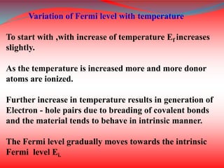
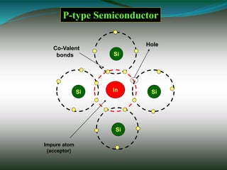
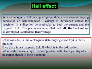
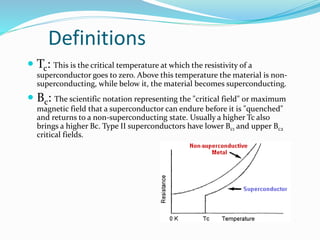
SlideShare a Scribd company logo
Advancements of Semiconductors
&Superconductors
Contents Semiconductor
 Types of Semiconductor
 Diagrams & Carrier Concentration
 Applications of Semiconductor
 Organic Semiconductor
 Superconductors
 Types of Semiconductor
 Meissner Effect
 Cooper Pair
 Application of Superconductors
 Economic Impact
 Advantages Semiconductor & Superconductors
Semiconductor
 Semiconductors are materials whose electronic
properties are intermediate between those of Metals and
Insulators.
 They have conductivities in the range of 10 -4 to 10
+4S/m.
 The interesting feature about semiconductors is that
they are bipolar and current is transported by two
charge carriers of opposite sign.
 These intermediate properties are determined by
1.Crystal Structure bonding Characteristics.
2.Electronic Energy bands.
 Silicon and Germanium are elemental semiconductors
and they have four valence electrons which are
distributed among the outermost S and p orbital's.
 These outer most S and p orbital's of Semiconductors
involve in Sp3 hybridanisation.
 These Sp3 orbital's form four covalent bonds of equal
angular separation leading to a tetrahedral arrangement
of atoms in space results tetrahedron shape, resulting
crystal structure is known as Diamond cubic crystal
structure
Semiconductors are mainly two types
1. Intrinsic (Pure) Semiconductors
2. Extrinsic (Impure) Semiconductors
Intrinsic Semiconductor
 A Semiconductor which does not have any kind of
impurities, behaves as an Insulator at 0k and behaves as a
Conductor at higher temperature is known as Intrinsic
Semiconductor or Pure Semiconductors.
 Germanium and Silicon (4th group elements) are the best
examples of intrinsic semiconductors and they possess
diamond cubic crystalline structure.
Si
Si
SiSiSi
Valence Cell
Covalent bonds
Intrinsic Semiconductor
E
Ef
Ev
Valence band
Ec
Conduction band
Ec
Electron
energy
Distance
KE of
Electron
= E - Ec
KE of Hole
=
Ev - E
Fermi energy level
Carrier Concentration in Intrinsic Semiconductor
When a suitable form of Energy is supplied to a
Semiconductor then electrons take transition from
Valence band to Conduction band.
Hence a free electron in Conduction band and
simultaneously free hole in Valence band is formed.
This phenomenon is known as Electron - Hole pair
generation.
In Intrinsic Semiconductor the Number of Conduction
electrons will be equal to the Number of Vacant sites or
holes in the valence band.
Extrinsic Semiconductors
 The Extrinsic Semiconductors are those in which impurities of
large quantity are present. Usually, the impurities can be either
3rd group elements or 5th group elements.
 Based on the impurities present in the Extrinsic
Semiconductors, they are classified into two categories.
1. N-type semiconductors
2. P-type semiconductors
When any pentavalent element such as Phosphorous,
Arsenic or Antimony is added to the intrinsic
Semiconductor , four electrons are involved in
covalent bonding with four neighboring pure
Semiconductor atoms.
The fifth electron is weakly bound to the parent
atom. And even for lesser thermal energy it is
released Leaving the parent atom positively ionized.
N - type
Semiconductors
N-type
Semiconductor
Si
Si
SiPSi
Free electron
Impure atom
(Donor)
The Intrinsic Semiconductors doped with pentavalent
impurities are called N-type Semiconductors.
The energy level of fifth electron is called donor level.
The donor level is close to the bottom of the conduction
band most of the donor level electrons are excited in to
the conduction band at room temperature and become
the Majority charge carriers.
Hence in N-type Semiconductors electrons are Majority
carriers and holes are Minority carriers.
E Ed
Ev
Valence band
Ec
Conduction band
Ec
Electron
energy
Distance
Donor levels
Eg
Carrier Concentration in N-type Semiconductor
 Consider Nd is the donor Concentration i.e., the
number of donor atoms per unit volume of the
material and Ed is the donor energy level.
 At very low temperatures all donor levels are filled
with electrons.
 With increase of temperature more and more donor
atoms get ionized and the density of electrons in the
conduction band increases.
Variation of Fermi level with temperature
To start with ,with increase of temperature Ef increases
slightly.
As the temperature is increased more and more donor
atoms are ionized.
Further increase in temperature results in generation of
Electron - hole pairs due to breading of covalent bonds
and the material tends to behave in intrinsic manner.
The Fermi level gradually moves towards the intrinsic
Fermi level Ei.
P-type semiconductors
 When a trivalent elements such as Al, Ga or Indium have
three electrons in their outer most orbits , added to the
intrinsic semiconductor all the three electrons of Indium are
engaged in covalent bonding with the three neighboring Si
atoms.
 Indium needs one more electron to complete its bond. this
electron maybe supplied by Silicon , there by creating a vacant
electron site or hole on the semiconductor atom.
 Indium accepts one extra electron, the energy level of this
impurity atom is called acceptor level and this acceptor level
lies just above the valence band.
 These type of trivalent impurities are called acceptor
impurities and the semiconductors doped the acceptor
impurities are called P-type semiconductors.
Si
Si
SiInSi
Hole
Co-Valent
bonds
Impure atom
(acceptor)
P-type Semiconductor
E
Ea
Ev
Valence band
Ec
Conduction band
Ec
Electron
energy
temperature
Acceptor levels
Eg
 Even at relatively low temperatures, these
acceptor atoms get ionized taking electrons
from valence band and thus giving rise to holes
in valence band for conduction.
 Due to ionization of acceptor atoms only holes
and no electrons are created.
 Thus holes are more in number than electrons
and hence holes are majority carriers and
electros are minority carriers in P-type
semiconductors.
Hall effect
When a magnetic field is applied perpendicular to a current carrying
conductor or semiconductor, voltage is developed across the
specimen in a direction perpendicular to both the current and the
magnetic field. This phenomenon is called the Hall effect and voltage
so developed is called the Hall voltage.
Let us consider, a thin rectangular slab carrying current (i) in the x-
direction.
If we place it in a magnetic field B which is in the y-direction.
Potential difference Vpq will develop between the faces p and q which
are perpendicular to the z-direction.
i
B
P
Q
X
Y
Z
+ + ++ +VH
+++++++
+ ++++++
+
++ + +
+
-
P – type semiconductor
i
B
X
Y
Z
VH
+
-
_
_ _
__ _
_
__ __
_ _
_
_
_
_ _ P
Q
N – type semiconductor
Applications
 Displays:
 (OLED) Organic Light Emitting Diodes
 RFID :
 Organic Nano-Radio Frequency Identification Devices
 Solar cells
 One of the biggest applications of organic
transistors right now.
Organic TFTs may be used to drive LCDs and potentially
even OLEDs, allowing integration of entire displays on
plastic.
 Brighter displays
 Thinner displays
 More flexible
Displays (OLED)
RFID
 Passive RF Devices that talk to the outside world …
so there will be no need for scanners.
RFID
benefits
 Quicker Checkout
 Improved Inventory Control
 Reduced Waste
 Efficient flow of goods from
manufacturer to consumer
Solar Cells
 The light falls on the polymer
 Electron/hole is generated
 The electron is captured C60
 The electricity is passed by the
nanotube
Future of Organic Semiconductor
 Smart Textiles
 Lab on a chip
 Portable compact screens
 Skin Cancer treatment
Organic Semiconductors
• Primary interest: Organic LEDs and displays.
• Low cost plastic electronics.
• Modification of semiconductor devices.
Polymers
Long molecular chains, „Spin-Coating“.
Monomers
Extended and conjugated -electron system.
Phthalocyanines, perylene derivatives.
Organic Molecular Beam Deposition (OMBD).
(S. R. Forrest, Chem. Rev. 97 (1997) 1793)
IHP Research Training Network G. Salvan,
TU Chemnitz
Organic semiconductors
Displays (Kodak)
Organic
field-effect transistors
GaAs(100)
Organic Interlayer
V
I
MetalOrganic/Inorganic
Microwave Diodes
Electrically driven
organic lasers
Organic-modified Schottky DiodesPlastic solar cells
An element, inter-metallic alloy, or compound that will
conduct electricity without resistance below a certain
temperature, magnetic field, and applied current.
Definition of Superconductor:
Definitions
 Tc: This is the critical temperature at which the resistivity of a
superconductor goes to zero. Above this temperature the material is non-
superconducting, while below it, the material becomes superconducting.
 Bc: The scientific notation representing the "critical field" or maximum
magnetic field that a superconductor can endure before it is "quenched"
and returns to a non-superconducting state. Usually a higher Tc also
brings a higher Bc. Type II superconductors have lower Bc1 and upper Bc2
critical fields.
Definitions
Jc: The scientific notation representing the "critical current
density" or maximum current that a superconductor can carry
without becoming non-superconductive.
 Meissner Effect: Exhibiting diamagnetic properties to the
total exclusion of all magnetic fields. (Named for Walter Meissner.)
This is a classic hallmark of superconductivity and can actually be
used to levitate a strong rare-earth magnet.
Superconductor Types
 Type I
Exhibits perfect diamagnetism below transition temperature Tc
and has only one critical magnetic field Bc.
 Type II
Totally expels and excludes magnetic flux below lower critical
field Bc1 and partially does so between Bc1 and upper critical
field Bc2; all superconductors except elements are Type II. This
type has a larger Tc than that of a Type I superconductor.
YBa2Cu307
 Discovered: 1987 by Paul Chu
 Tc: 90-95K
 Bc2: 100 Tesla at 77 K
 Jc: 1.0x10⁹ A/m2 at 77 K
 Referred to as “1-2-3” superconductor
because of the ratio of the three metallic
elements
 Type: Type II Ceramic
The Meissner Effect
 Levitation of a magnet above a cooled superconductor, the
Meissner Effect, has been well known for many years. If a
superconductor is cooled below its critical temperature
while in a magnetic field, the magnetic field surrounds but
does not penetrate the superconductor. The magnet
induces current in the superconductor which creates a
counter-magnetic force that causes the two materials to
repel. This can be seen as the magnet is levitated above the
superconductor.
Superconductivity is an exciting field of
physics! Picture below is the levitation of a magnet above a cooled
superconductor, the Meissner Effect
Cooper Pair:
 Two electrons that appear to "team up" in accordance
with theory - BCS or other - despite the fact that they
both have a negative charge and normally repel each
other. Below the superconducting transition
temperature, paired electrons form a condensate - a
macroscopically occupied single quantum state -
which flows without resistance
Cooper pairs:
SQUIDS
Economic Impact of
Superconducting Equipment
• Utilities
• Higher density transmission uses & higher
economic productivity
• Reduced environmental impact
• Industrial
More cost effective industrial processes:
• Manufacturing & energy production
• Electrical storage, transmission and expansion
• Transportation
More cost effective electrical transportation:
• High Speed Rail & MAGLEV technologies
• Electric car / bus
• Ship
Application of Superconductors
•Particle Accelerators
•Generators
•Transportation
•Power Transmission
•Electric Motors
•Military
•Computing
•Medical
•B Field Detection (SQUIDS)
The Yamanashi MLX01 MagLev train
Semiconductors
a semiconductor device on changing temperature can be used as a
conductor as well as an insulator. This is the main advantage of a
semiconductor device.it is also light weight, small, cheap and finds many
applications in modern devices like computers, electrical appliances.
Superconductors
Can carry large quanities of energy without heat loss and are able
to generate strong magnetic fields. Superconductors beneficial applications
in medical imaging techniques. New superconductive films may result in
miniaturization and increased speed in computer chips.
Advantages of Semiconductors & Superconductors
Levitating train can travel at >300 mph!
Any Questions?
Suba Shree B
Sudharsana Devi K

More Related Content

What's hot

Semiconductor Devices
Semiconductor DevicesSemiconductor Devices
Semiconductor Devices
Rajesh Kumar
 
semiconductor - description and application
semiconductor - description and applicationsemiconductor - description and application
semiconductor - description and application
BishnupadaSarkar2
 
PN JUNCTION
PN JUNCTION PN JUNCTION
PN JUNCTION
Mehedi Hasan
 
EDC ( P-type & N-type )
EDC ( P-type & N-type )EDC ( P-type & N-type )
EDC ( P-type & N-type )
Pritam Shil
 
LED
LEDLED
Band theory of solid
Band theory of solidBand theory of solid
Band theory of solid
Keyur Patel
 
SEMICONDUCTOR PHYSICS
SEMICONDUCTOR PHYSICSSEMICONDUCTOR PHYSICS
SEMICONDUCTOR PHYSICS
Vaishnavi Bathina
 
Conductor semiconductor insulator
Conductor semiconductor insulatorConductor semiconductor insulator
Conductor semiconductor insulator
ravikumar s
 
A BASIC INTRODUCTION TO SEMICONDUCTOR DEVICES - THE
A BASIC INTRODUCTION TO SEMICONDUCTOR DEVICES - THEA BASIC INTRODUCTION TO SEMICONDUCTOR DEVICES - THE
A BASIC INTRODUCTION TO SEMICONDUCTOR DEVICES - THEWinston Bent A.S.S.
 
Light Emitting Diode Presentation Report
Light Emitting Diode  Presentation ReportLight Emitting Diode  Presentation Report
Light Emitting Diode Presentation Report
Devansh Gupta
 
Introduction to semiconductor materials
Introduction to semiconductor materialsIntroduction to semiconductor materials
Introduction to semiconductor materialsDr. Ghanshyam Singh
 
PHYSICS OF SEMICONDUCTOR DEVICES
PHYSICS OF SEMICONDUCTOR DEVICESPHYSICS OF SEMICONDUCTOR DEVICES
PHYSICS OF SEMICONDUCTOR DEVICES
Vaishnavi Bathina
 
Semiconductor devices
Semiconductor devicesSemiconductor devices
Semiconductor devices
GS Virdi
 
semiconductors ppt
semiconductors pptsemiconductors ppt
semiconductors ppt
vagdevi kuntla
 
Diode v i characteristic
Diode v i characteristicDiode v i characteristic
Diode v i characteristic
Unsa Shakir
 
Tunnel diode
Tunnel diodeTunnel diode
Tunnel diode
Sheikh Danish
 
Half wave Rectifier & Full wave Rectifier with their descriptions.
Half wave Rectifier & Full wave Rectifier with their descriptions.Half wave Rectifier & Full wave Rectifier with their descriptions.
Half wave Rectifier & Full wave Rectifier with their descriptions.
Deepanjana Paul
 
Semiconductor diodes
Semiconductor diodesSemiconductor diodes
Semiconductor diodes
priyanka singh
 
BAND THEORY OF SOLIDS
BAND THEORY OF SOLIDSBAND THEORY OF SOLIDS
BAND THEORY OF SOLIDSMahi Shinde
 

What's hot (20)

Semiconductor Devices
Semiconductor DevicesSemiconductor Devices
Semiconductor Devices
 
semiconductor - description and application
semiconductor - description and applicationsemiconductor - description and application
semiconductor - description and application
 
PN JUNCTION
PN JUNCTION PN JUNCTION
PN JUNCTION
 
EDC ( P-type & N-type )
EDC ( P-type & N-type )EDC ( P-type & N-type )
EDC ( P-type & N-type )
 
LED
LEDLED
LED
 
Band theory of solid
Band theory of solidBand theory of solid
Band theory of solid
 
SEMICONDUCTOR PHYSICS
SEMICONDUCTOR PHYSICSSEMICONDUCTOR PHYSICS
SEMICONDUCTOR PHYSICS
 
Conductor semiconductor insulator
Conductor semiconductor insulatorConductor semiconductor insulator
Conductor semiconductor insulator
 
A BASIC INTRODUCTION TO SEMICONDUCTOR DEVICES - THE
A BASIC INTRODUCTION TO SEMICONDUCTOR DEVICES - THEA BASIC INTRODUCTION TO SEMICONDUCTOR DEVICES - THE
A BASIC INTRODUCTION TO SEMICONDUCTOR DEVICES - THE
 
Light Emitting Diode Presentation Report
Light Emitting Diode  Presentation ReportLight Emitting Diode  Presentation Report
Light Emitting Diode Presentation Report
 
Introduction to semiconductor materials
Introduction to semiconductor materialsIntroduction to semiconductor materials
Introduction to semiconductor materials
 
Semiconductor physics
Semiconductor physicsSemiconductor physics
Semiconductor physics
 
PHYSICS OF SEMICONDUCTOR DEVICES
PHYSICS OF SEMICONDUCTOR DEVICESPHYSICS OF SEMICONDUCTOR DEVICES
PHYSICS OF SEMICONDUCTOR DEVICES
 
Semiconductor devices
Semiconductor devicesSemiconductor devices
Semiconductor devices
 
semiconductors ppt
semiconductors pptsemiconductors ppt
semiconductors ppt
 
Diode v i characteristic
Diode v i characteristicDiode v i characteristic
Diode v i characteristic
 
Tunnel diode
Tunnel diodeTunnel diode
Tunnel diode
 
Half wave Rectifier & Full wave Rectifier with their descriptions.
Half wave Rectifier & Full wave Rectifier with their descriptions.Half wave Rectifier & Full wave Rectifier with their descriptions.
Half wave Rectifier & Full wave Rectifier with their descriptions.
 
Semiconductor diodes
Semiconductor diodesSemiconductor diodes
Semiconductor diodes
 
BAND THEORY OF SOLIDS
BAND THEORY OF SOLIDSBAND THEORY OF SOLIDS
BAND THEORY OF SOLIDS
 

Viewers also liked

Study of charge transport mechanism in organic and organicinorganic hybrid sy...
Study of charge transport mechanism in organic and organicinorganic hybrid sy...Study of charge transport mechanism in organic and organicinorganic hybrid sy...
Study of charge transport mechanism in organic and organicinorganic hybrid sy...
Tauqueer Khan
 
The Role of Molecular Structure and Conformation in Polymer Opto-Electronics
The Role of Molecular Structure and Conformation in Polymer Opto-ElectronicsThe Role of Molecular Structure and Conformation in Polymer Opto-Electronics
The Role of Molecular Structure and Conformation in Polymer Opto-Electronics
cdtpv
 
Organic Semiconductor Technology
Organic Semiconductor TechnologyOrganic Semiconductor Technology
Organic Semiconductor Technologysamiseecs
 
Solar Cells Lecture 5: Organic Photovoltaics
Solar Cells Lecture 5: Organic PhotovoltaicsSolar Cells Lecture 5: Organic Photovoltaics
Solar Cells Lecture 5: Organic Photovoltaics
Tuong Do
 
Physics semiconductors project
Physics semiconductors projectPhysics semiconductors project
Physics semiconductors project
Aashirwad Jindal
 
Systematic, toolchain JS
Systematic, toolchain JSSystematic, toolchain JS
Systematic, toolchain JS
Raphaël Boucher
 
DHW Planning for Growth copy
DHW Planning for Growth copyDHW Planning for Growth copy
DHW Planning for Growth copyBrett Lear
 
Mk0017 e-marketing
Mk0017 e-marketingMk0017 e-marketing
Mk0017 e-marketing
consult4solutions
 
Pm0015 quantitaive methods in project management
Pm0015 quantitaive methods in project managementPm0015 quantitaive methods in project management
Pm0015 quantitaive methods in project management
consult4solutions
 
Access control basics-2
Access control basics-2Access control basics-2
Access control basics-2
grantlerc
 
Wizard Food: sweets, butterbeer, and childhood tastes
Wizard Food: sweets, butterbeer, and childhood tastesWizard Food: sweets, butterbeer, and childhood tastes
Wizard Food: sweets, butterbeer, and childhood tastes
Emily Truman
 
Otek crm destek
Otek crm destekOtek crm destek
Otek crm destek
Caner Kıvam
 
6. tres buenas prácticas agrícolas interrelacionadas que condicionan la produ...
6. tres buenas prácticas agrícolas interrelacionadas que condicionan la produ...6. tres buenas prácticas agrícolas interrelacionadas que condicionan la produ...
6. tres buenas prácticas agrícolas interrelacionadas que condicionan la produ...
Ana Martinez
 
Mb0052 strategic management and business policy
Mb0052 strategic management and business policyMb0052 strategic management and business policy
Mb0052 strategic management and business policy
consult4solutions
 
Trabajos de los informes de word
Trabajos de los informes de wordTrabajos de los informes de word
Trabajos de los informes de word
stalingeo
 
ЗЕЙНЕТАҚЬI ЗАҢНАМАСЬIНДАҒЬI ЖАҢАЛЬIҚТАР
ЗЕЙНЕТАҚЬI ЗАҢНАМАСЬIНДАҒЬI ЖАҢАЛЬIҚТАРЗЕЙНЕТАҚЬI ЗАҢНАМАСЬIНДАҒЬI ЖАҢАЛЬIҚТАР
ЗЕЙНЕТАҚЬI ЗАҢНАМАСЬIНДАҒЬI ЖАҢАЛЬIҚТАР
Yelnur Shalkibayev
 

Viewers also liked (20)

Study of charge transport mechanism in organic and organicinorganic hybrid sy...
Study of charge transport mechanism in organic and organicinorganic hybrid sy...Study of charge transport mechanism in organic and organicinorganic hybrid sy...
Study of charge transport mechanism in organic and organicinorganic hybrid sy...
 
The Role of Molecular Structure and Conformation in Polymer Opto-Electronics
The Role of Molecular Structure and Conformation in Polymer Opto-ElectronicsThe Role of Molecular Structure and Conformation in Polymer Opto-Electronics
The Role of Molecular Structure and Conformation in Polymer Opto-Electronics
 
Organic Semiconductor Technology
Organic Semiconductor TechnologyOrganic Semiconductor Technology
Organic Semiconductor Technology
 
Semiconductors
SemiconductorsSemiconductors
Semiconductors
 
Solar Cells Lecture 5: Organic Photovoltaics
Solar Cells Lecture 5: Organic PhotovoltaicsSolar Cells Lecture 5: Organic Photovoltaics
Solar Cells Lecture 5: Organic Photovoltaics
 
Transportation ppt
Transportation pptTransportation ppt
Transportation ppt
 
Physics semiconductors project
Physics semiconductors projectPhysics semiconductors project
Physics semiconductors project
 
Systematic, toolchain JS
Systematic, toolchain JSSystematic, toolchain JS
Systematic, toolchain JS
 
DHW Planning for Growth copy
DHW Planning for Growth copyDHW Planning for Growth copy
DHW Planning for Growth copy
 
Mk0017 e-marketing
Mk0017 e-marketingMk0017 e-marketing
Mk0017 e-marketing
 
Pm0015 quantitaive methods in project management
Pm0015 quantitaive methods in project managementPm0015 quantitaive methods in project management
Pm0015 quantitaive methods in project management
 
Access control basics-2
Access control basics-2Access control basics-2
Access control basics-2
 
Wizard Food: sweets, butterbeer, and childhood tastes
Wizard Food: sweets, butterbeer, and childhood tastesWizard Food: sweets, butterbeer, and childhood tastes
Wizard Food: sweets, butterbeer, and childhood tastes
 
Otek crm destek
Otek crm destekOtek crm destek
Otek crm destek
 
t_mashapa[1]
t_mashapa[1]t_mashapa[1]
t_mashapa[1]
 
6. tres buenas prácticas agrícolas interrelacionadas que condicionan la produ...
6. tres buenas prácticas agrícolas interrelacionadas que condicionan la produ...6. tres buenas prácticas agrícolas interrelacionadas que condicionan la produ...
6. tres buenas prácticas agrícolas interrelacionadas que condicionan la produ...
 
Hip Hop
Hip HopHip Hop
Hip Hop
 
Mb0052 strategic management and business policy
Mb0052 strategic management and business policyMb0052 strategic management and business policy
Mb0052 strategic management and business policy
 
Trabajos de los informes de word
Trabajos de los informes de wordTrabajos de los informes de word
Trabajos de los informes de word
 
ЗЕЙНЕТАҚЬI ЗАҢНАМАСЬIНДАҒЬI ЖАҢАЛЬIҚТАР
ЗЕЙНЕТАҚЬI ЗАҢНАМАСЬIНДАҒЬI ЖАҢАЛЬIҚТАРЗЕЙНЕТАҚЬI ЗАҢНАМАСЬIНДАҒЬI ЖАҢАЛЬIҚТАР
ЗЕЙНЕТАҚЬI ЗАҢНАМАСЬIНДАҒЬI ЖАҢАЛЬIҚТАР
 

Similar to Ppt semi conductor

Advancements of Semi conductors and Superconductors
Advancements of Semi conductors and SuperconductorsAdvancements of Semi conductors and Superconductors
Advancements of Semi conductors and Superconductors
adnanalvi051
 
M.Sc_._III_Sem_Chemistry_SUPERCONDUCTORS_Dr._Anshumala_Vani.pdf
M.Sc_._III_Sem_Chemistry_SUPERCONDUCTORS_Dr._Anshumala_Vani.pdfM.Sc_._III_Sem_Chemistry_SUPERCONDUCTORS_Dr._Anshumala_Vani.pdf
M.Sc_._III_Sem_Chemistry_SUPERCONDUCTORS_Dr._Anshumala_Vani.pdf
rajpurohitritu123
 
Semi conductor materials.pptx
Semi conductor materials.pptxSemi conductor materials.pptx
Semi conductor materials.pptx
AliRaZaAnsari13
 
Semiconductor devices specialization
Semiconductor devices  specializationSemiconductor devices  specialization
Semiconductor devices specialization
Abhishek Sur
 
B.tech sem i engineering physics u ii chapter 1-band theory of solid
B.tech sem i engineering physics u ii chapter 1-band theory of solidB.tech sem i engineering physics u ii chapter 1-band theory of solid
B.tech sem i engineering physics u ii chapter 1-band theory of solid
Rai University
 
Energy conversion & physics of semiconductors
Energy conversion & physics of semiconductorsEnergy conversion & physics of semiconductors
Energy conversion & physics of semiconductors
Maulik Ramani
 
semiconductor and hall effect.pptx chemistry .....
semiconductor and hall effect.pptx chemistry .....semiconductor and hall effect.pptx chemistry .....
semiconductor and hall effect.pptx chemistry .....
amruthatk3
 
B.Tech sem I Engineering Physics U-II Chapter 1-Band theory of solid
B.Tech sem I Engineering Physics U-II Chapter 1-Band theory of solidB.Tech sem I Engineering Physics U-II Chapter 1-Band theory of solid
B.Tech sem I Engineering Physics U-II Chapter 1-Band theory of solid
Abhi Hirpara
 
Class 12 th semiconductor part 2
Class 12 th semiconductor part 2Class 12 th semiconductor part 2
Class 12 th semiconductor part 2
Priyanka Jakhar
 
device chemistry.pptx
device chemistry.pptxdevice chemistry.pptx
device chemistry.pptx
Vinay625532
 
Semiconductor Devices.pptx
Semiconductor Devices.pptxSemiconductor Devices.pptx
Semiconductor Devices.pptx
ssuser8984f3
 
MODULE 1 modified - CET (1).pptx
MODULE 1 modified - CET (1).pptxMODULE 1 modified - CET (1).pptx
MODULE 1 modified - CET (1).pptx
KerenElisheba
 
BASIC ELECTRONICS on physics for teaching grade 12
BASIC ELECTRONICS on physics for teaching grade 12BASIC ELECTRONICS on physics for teaching grade 12
BASIC ELECTRONICS on physics for teaching grade 12
JerryOgugo
 
yfliyfuyfyfyfyfifif Semiconductors-PPT.pptx
yfliyfuyfyfyfyfifif Semiconductors-PPT.pptxyfliyfuyfyfyfyfifif Semiconductors-PPT.pptx
yfliyfuyfyfyfyfifif Semiconductors-PPT.pptx
praveenkammar9
 
BEEME UNIT IV.ppt
BEEME UNIT IV.pptBEEME UNIT IV.ppt
BEEME UNIT IV.ppt
Karthik Kathan
 
SEMICONDUCTORS ppt.pptx
SEMICONDUCTORS ppt.pptxSEMICONDUCTORS ppt.pptx
SEMICONDUCTORS ppt.pptx
SayantaniBose2
 
Material engineering and its applications.
Material engineering and its applications.Material engineering and its applications.
Material engineering and its applications.
Omkar Rane
 
CSE-AE.pptx
CSE-AE.pptxCSE-AE.pptx
CSE-AE.pptx
anitha5075
 
Electronic
ElectronicElectronic
Electronic
HarisKhan918416
 
Diploma sem 2 applied science physics-unit 3-chap-1 band theory of solid
Diploma sem 2 applied science physics-unit 3-chap-1 band theory of solidDiploma sem 2 applied science physics-unit 3-chap-1 band theory of solid
Diploma sem 2 applied science physics-unit 3-chap-1 band theory of solid
Rai University
 

Similar to Ppt semi conductor (20)

Advancements of Semi conductors and Superconductors
Advancements of Semi conductors and SuperconductorsAdvancements of Semi conductors and Superconductors
Advancements of Semi conductors and Superconductors
 
M.Sc_._III_Sem_Chemistry_SUPERCONDUCTORS_Dr._Anshumala_Vani.pdf
M.Sc_._III_Sem_Chemistry_SUPERCONDUCTORS_Dr._Anshumala_Vani.pdfM.Sc_._III_Sem_Chemistry_SUPERCONDUCTORS_Dr._Anshumala_Vani.pdf
M.Sc_._III_Sem_Chemistry_SUPERCONDUCTORS_Dr._Anshumala_Vani.pdf
 
Semi conductor materials.pptx
Semi conductor materials.pptxSemi conductor materials.pptx
Semi conductor materials.pptx
 
Semiconductor devices specialization
Semiconductor devices  specializationSemiconductor devices  specialization
Semiconductor devices specialization
 
B.tech sem i engineering physics u ii chapter 1-band theory of solid
B.tech sem i engineering physics u ii chapter 1-band theory of solidB.tech sem i engineering physics u ii chapter 1-band theory of solid
B.tech sem i engineering physics u ii chapter 1-band theory of solid
 
Energy conversion & physics of semiconductors
Energy conversion & physics of semiconductorsEnergy conversion & physics of semiconductors
Energy conversion & physics of semiconductors
 
semiconductor and hall effect.pptx chemistry .....
semiconductor and hall effect.pptx chemistry .....semiconductor and hall effect.pptx chemistry .....
semiconductor and hall effect.pptx chemistry .....
 
B.Tech sem I Engineering Physics U-II Chapter 1-Band theory of solid
B.Tech sem I Engineering Physics U-II Chapter 1-Band theory of solidB.Tech sem I Engineering Physics U-II Chapter 1-Band theory of solid
B.Tech sem I Engineering Physics U-II Chapter 1-Band theory of solid
 
Class 12 th semiconductor part 2
Class 12 th semiconductor part 2Class 12 th semiconductor part 2
Class 12 th semiconductor part 2
 
device chemistry.pptx
device chemistry.pptxdevice chemistry.pptx
device chemistry.pptx
 
Semiconductor Devices.pptx
Semiconductor Devices.pptxSemiconductor Devices.pptx
Semiconductor Devices.pptx
 
MODULE 1 modified - CET (1).pptx
MODULE 1 modified - CET (1).pptxMODULE 1 modified - CET (1).pptx
MODULE 1 modified - CET (1).pptx
 
BASIC ELECTRONICS on physics for teaching grade 12
BASIC ELECTRONICS on physics for teaching grade 12BASIC ELECTRONICS on physics for teaching grade 12
BASIC ELECTRONICS on physics for teaching grade 12
 
yfliyfuyfyfyfyfifif Semiconductors-PPT.pptx
yfliyfuyfyfyfyfifif Semiconductors-PPT.pptxyfliyfuyfyfyfyfifif Semiconductors-PPT.pptx
yfliyfuyfyfyfyfifif Semiconductors-PPT.pptx
 
BEEME UNIT IV.ppt
BEEME UNIT IV.pptBEEME UNIT IV.ppt
BEEME UNIT IV.ppt
 
SEMICONDUCTORS ppt.pptx
SEMICONDUCTORS ppt.pptxSEMICONDUCTORS ppt.pptx
SEMICONDUCTORS ppt.pptx
 
Material engineering and its applications.
Material engineering and its applications.Material engineering and its applications.
Material engineering and its applications.
 
CSE-AE.pptx
CSE-AE.pptxCSE-AE.pptx
CSE-AE.pptx
 
Electronic
ElectronicElectronic
Electronic
 
Diploma sem 2 applied science physics-unit 3-chap-1 band theory of solid
Diploma sem 2 applied science physics-unit 3-chap-1 band theory of solidDiploma sem 2 applied science physics-unit 3-chap-1 band theory of solid
Diploma sem 2 applied science physics-unit 3-chap-1 band theory of solid
 

Recently uploaded

Travis Hills' Endeavors in Minnesota: Fostering Environmental and Economic Pr...
Travis Hills' Endeavors in Minnesota: Fostering Environmental and Economic Pr...Travis Hills' Endeavors in Minnesota: Fostering Environmental and Economic Pr...
Travis Hills' Endeavors in Minnesota: Fostering Environmental and Economic Pr...
Travis Hills MN
 
原版制作(carleton毕业证书)卡尔顿大学毕业证硕士文凭原版一模一样
原版制作(carleton毕业证书)卡尔顿大学毕业证硕士文凭原版一模一样原版制作(carleton毕业证书)卡尔顿大学毕业证硕士文凭原版一模一样
原版制作(carleton毕业证书)卡尔顿大学毕业证硕士文凭原版一模一样
yqqaatn0
 
The use of Nauplii and metanauplii artemia in aquaculture (brine shrimp).pptx
The use of Nauplii and metanauplii artemia in aquaculture (brine shrimp).pptxThe use of Nauplii and metanauplii artemia in aquaculture (brine shrimp).pptx
The use of Nauplii and metanauplii artemia in aquaculture (brine shrimp).pptx
MAGOTI ERNEST
 
Earliest Galaxies in the JADES Origins Field: Luminosity Function and Cosmic ...
Earliest Galaxies in the JADES Origins Field: Luminosity Function and Cosmic ...Earliest Galaxies in the JADES Origins Field: Luminosity Function and Cosmic ...
Earliest Galaxies in the JADES Origins Field: Luminosity Function and Cosmic ...
Sérgio Sacani
 
Leaf Initiation, Growth and Differentiation.pdf
Leaf Initiation, Growth and Differentiation.pdfLeaf Initiation, Growth and Differentiation.pdf
Leaf Initiation, Growth and Differentiation.pdf
RenuJangid3
 
Nucleic Acid-its structural and functional complexity.
Nucleic Acid-its structural and functional complexity.Nucleic Acid-its structural and functional complexity.
Nucleic Acid-its structural and functional complexity.
Nistarini College, Purulia (W.B) India
 
Toxic effects of heavy metals : Lead and Arsenic
Toxic effects of heavy metals : Lead and ArsenicToxic effects of heavy metals : Lead and Arsenic
Toxic effects of heavy metals : Lead and Arsenic
sanjana502982
 
Orion Air Quality Monitoring Systems - CWS
Orion Air Quality Monitoring Systems - CWSOrion Air Quality Monitoring Systems - CWS
Orion Air Quality Monitoring Systems - CWS
Columbia Weather Systems
 
Unveiling the Energy Potential of Marshmallow Deposits.pdf
Unveiling the Energy Potential of Marshmallow Deposits.pdfUnveiling the Energy Potential of Marshmallow Deposits.pdf
Unveiling the Energy Potential of Marshmallow Deposits.pdf
Erdal Coalmaker
 
THEMATIC APPERCEPTION TEST(TAT) cognitive abilities, creativity, and critic...
THEMATIC  APPERCEPTION  TEST(TAT) cognitive abilities, creativity, and critic...THEMATIC  APPERCEPTION  TEST(TAT) cognitive abilities, creativity, and critic...
THEMATIC APPERCEPTION TEST(TAT) cognitive abilities, creativity, and critic...
Abdul Wali Khan University Mardan,kP,Pakistan
 
In silico drugs analogue design: novobiocin analogues.pptx
In silico drugs analogue design: novobiocin analogues.pptxIn silico drugs analogue design: novobiocin analogues.pptx
In silico drugs analogue design: novobiocin analogues.pptx
AlaminAfendy1
 
Phenomics assisted breeding in crop improvement
Phenomics assisted breeding in crop improvementPhenomics assisted breeding in crop improvement
Phenomics assisted breeding in crop improvement
IshaGoswami9
 
SAR of Medicinal Chemistry 1st by dk.pdf
SAR of Medicinal Chemistry 1st by dk.pdfSAR of Medicinal Chemistry 1st by dk.pdf
SAR of Medicinal Chemistry 1st by dk.pdf
KrushnaDarade1
 
PRESENTATION ABOUT PRINCIPLE OF COSMATIC EVALUATION
PRESENTATION ABOUT PRINCIPLE OF COSMATIC EVALUATIONPRESENTATION ABOUT PRINCIPLE OF COSMATIC EVALUATION
PRESENTATION ABOUT PRINCIPLE OF COSMATIC EVALUATION
ChetanK57
 
What is greenhouse gasses and how many gasses are there to affect the Earth.
What is greenhouse gasses and how many gasses are there to affect the Earth.What is greenhouse gasses and how many gasses are there to affect the Earth.
What is greenhouse gasses and how many gasses are there to affect the Earth.
moosaasad1975
 
bordetella pertussis.................................ppt
bordetella pertussis.................................pptbordetella pertussis.................................ppt
bordetella pertussis.................................ppt
kejapriya1
 
Deep Behavioral Phenotyping in Systems Neuroscience for Functional Atlasing a...
Deep Behavioral Phenotyping in Systems Neuroscience for Functional Atlasing a...Deep Behavioral Phenotyping in Systems Neuroscience for Functional Atlasing a...
Deep Behavioral Phenotyping in Systems Neuroscience for Functional Atlasing a...
Ana Luísa Pinho
 
Shallowest Oil Discovery of Turkiye.pptx
Shallowest Oil Discovery of Turkiye.pptxShallowest Oil Discovery of Turkiye.pptx
Shallowest Oil Discovery of Turkiye.pptx
Gokturk Mehmet Dilci
 
如何办理(uvic毕业证书)维多利亚大学毕业证本科学位证书原版一模一样
如何办理(uvic毕业证书)维多利亚大学毕业证本科学位证书原版一模一样如何办理(uvic毕业证书)维多利亚大学毕业证本科学位证书原版一模一样
如何办理(uvic毕业证书)维多利亚大学毕业证本科学位证书原版一模一样
yqqaatn0
 
Observation of Io’s Resurfacing via Plume Deposition Using Ground-based Adapt...
Observation of Io’s Resurfacing via Plume Deposition Using Ground-based Adapt...Observation of Io’s Resurfacing via Plume Deposition Using Ground-based Adapt...
Observation of Io’s Resurfacing via Plume Deposition Using Ground-based Adapt...
Sérgio Sacani
 

Recently uploaded (20)

Travis Hills' Endeavors in Minnesota: Fostering Environmental and Economic Pr...
Travis Hills' Endeavors in Minnesota: Fostering Environmental and Economic Pr...Travis Hills' Endeavors in Minnesota: Fostering Environmental and Economic Pr...
Travis Hills' Endeavors in Minnesota: Fostering Environmental and Economic Pr...
 
原版制作(carleton毕业证书)卡尔顿大学毕业证硕士文凭原版一模一样
原版制作(carleton毕业证书)卡尔顿大学毕业证硕士文凭原版一模一样原版制作(carleton毕业证书)卡尔顿大学毕业证硕士文凭原版一模一样
原版制作(carleton毕业证书)卡尔顿大学毕业证硕士文凭原版一模一样
 
The use of Nauplii and metanauplii artemia in aquaculture (brine shrimp).pptx
The use of Nauplii and metanauplii artemia in aquaculture (brine shrimp).pptxThe use of Nauplii and metanauplii artemia in aquaculture (brine shrimp).pptx
The use of Nauplii and metanauplii artemia in aquaculture (brine shrimp).pptx
 
Earliest Galaxies in the JADES Origins Field: Luminosity Function and Cosmic ...
Earliest Galaxies in the JADES Origins Field: Luminosity Function and Cosmic ...Earliest Galaxies in the JADES Origins Field: Luminosity Function and Cosmic ...
Earliest Galaxies in the JADES Origins Field: Luminosity Function and Cosmic ...
 
Leaf Initiation, Growth and Differentiation.pdf
Leaf Initiation, Growth and Differentiation.pdfLeaf Initiation, Growth and Differentiation.pdf
Leaf Initiation, Growth and Differentiation.pdf
 
Nucleic Acid-its structural and functional complexity.
Nucleic Acid-its structural and functional complexity.Nucleic Acid-its structural and functional complexity.
Nucleic Acid-its structural and functional complexity.
 
Toxic effects of heavy metals : Lead and Arsenic
Toxic effects of heavy metals : Lead and ArsenicToxic effects of heavy metals : Lead and Arsenic
Toxic effects of heavy metals : Lead and Arsenic
 
Orion Air Quality Monitoring Systems - CWS
Orion Air Quality Monitoring Systems - CWSOrion Air Quality Monitoring Systems - CWS
Orion Air Quality Monitoring Systems - CWS
 
Unveiling the Energy Potential of Marshmallow Deposits.pdf
Unveiling the Energy Potential of Marshmallow Deposits.pdfUnveiling the Energy Potential of Marshmallow Deposits.pdf
Unveiling the Energy Potential of Marshmallow Deposits.pdf
 
THEMATIC APPERCEPTION TEST(TAT) cognitive abilities, creativity, and critic...
THEMATIC  APPERCEPTION  TEST(TAT) cognitive abilities, creativity, and critic...THEMATIC  APPERCEPTION  TEST(TAT) cognitive abilities, creativity, and critic...
THEMATIC APPERCEPTION TEST(TAT) cognitive abilities, creativity, and critic...
 
In silico drugs analogue design: novobiocin analogues.pptx
In silico drugs analogue design: novobiocin analogues.pptxIn silico drugs analogue design: novobiocin analogues.pptx
In silico drugs analogue design: novobiocin analogues.pptx
 
Phenomics assisted breeding in crop improvement
Phenomics assisted breeding in crop improvementPhenomics assisted breeding in crop improvement
Phenomics assisted breeding in crop improvement
 
SAR of Medicinal Chemistry 1st by dk.pdf
SAR of Medicinal Chemistry 1st by dk.pdfSAR of Medicinal Chemistry 1st by dk.pdf
SAR of Medicinal Chemistry 1st by dk.pdf
 
PRESENTATION ABOUT PRINCIPLE OF COSMATIC EVALUATION
PRESENTATION ABOUT PRINCIPLE OF COSMATIC EVALUATIONPRESENTATION ABOUT PRINCIPLE OF COSMATIC EVALUATION
PRESENTATION ABOUT PRINCIPLE OF COSMATIC EVALUATION
 
What is greenhouse gasses and how many gasses are there to affect the Earth.
What is greenhouse gasses and how many gasses are there to affect the Earth.What is greenhouse gasses and how many gasses are there to affect the Earth.
What is greenhouse gasses and how many gasses are there to affect the Earth.
 
bordetella pertussis.................................ppt
bordetella pertussis.................................pptbordetella pertussis.................................ppt
bordetella pertussis.................................ppt
 
Deep Behavioral Phenotyping in Systems Neuroscience for Functional Atlasing a...
Deep Behavioral Phenotyping in Systems Neuroscience for Functional Atlasing a...Deep Behavioral Phenotyping in Systems Neuroscience for Functional Atlasing a...
Deep Behavioral Phenotyping in Systems Neuroscience for Functional Atlasing a...
 
Shallowest Oil Discovery of Turkiye.pptx
Shallowest Oil Discovery of Turkiye.pptxShallowest Oil Discovery of Turkiye.pptx
Shallowest Oil Discovery of Turkiye.pptx
 
如何办理(uvic毕业证书)维多利亚大学毕业证本科学位证书原版一模一样
如何办理(uvic毕业证书)维多利亚大学毕业证本科学位证书原版一模一样如何办理(uvic毕业证书)维多利亚大学毕业证本科学位证书原版一模一样
如何办理(uvic毕业证书)维多利亚大学毕业证本科学位证书原版一模一样
 
Observation of Io’s Resurfacing via Plume Deposition Using Ground-based Adapt...
Observation of Io’s Resurfacing via Plume Deposition Using Ground-based Adapt...Observation of Io’s Resurfacing via Plume Deposition Using Ground-based Adapt...
Observation of Io’s Resurfacing via Plume Deposition Using Ground-based Adapt...
 

Ppt semi conductor

  • 1.
  • 3. Contents Semiconductor  Types of Semiconductor  Diagrams & Carrier Concentration  Applications of Semiconductor  Organic Semiconductor  Superconductors  Types of Semiconductor  Meissner Effect  Cooper Pair  Application of Superconductors  Economic Impact  Advantages Semiconductor & Superconductors
  • 4. Semiconductor  Semiconductors are materials whose electronic properties are intermediate between those of Metals and Insulators.  They have conductivities in the range of 10 -4 to 10 +4S/m.  The interesting feature about semiconductors is that they are bipolar and current is transported by two charge carriers of opposite sign.  These intermediate properties are determined by 1.Crystal Structure bonding Characteristics. 2.Electronic Energy bands.
  • 5.  Silicon and Germanium are elemental semiconductors and they have four valence electrons which are distributed among the outermost S and p orbital's.  These outer most S and p orbital's of Semiconductors involve in Sp3 hybridanisation.  These Sp3 orbital's form four covalent bonds of equal angular separation leading to a tetrahedral arrangement of atoms in space results tetrahedron shape, resulting crystal structure is known as Diamond cubic crystal structure
  • 6. Semiconductors are mainly two types 1. Intrinsic (Pure) Semiconductors 2. Extrinsic (Impure) Semiconductors
  • 7. Intrinsic Semiconductor  A Semiconductor which does not have any kind of impurities, behaves as an Insulator at 0k and behaves as a Conductor at higher temperature is known as Intrinsic Semiconductor or Pure Semiconductors.  Germanium and Silicon (4th group elements) are the best examples of intrinsic semiconductors and they possess diamond cubic crystalline structure.
  • 9. E Ef Ev Valence band Ec Conduction band Ec Electron energy Distance KE of Electron = E - Ec KE of Hole = Ev - E Fermi energy level
  • 10. Carrier Concentration in Intrinsic Semiconductor When a suitable form of Energy is supplied to a Semiconductor then electrons take transition from Valence band to Conduction band. Hence a free electron in Conduction band and simultaneously free hole in Valence band is formed. This phenomenon is known as Electron - Hole pair generation. In Intrinsic Semiconductor the Number of Conduction electrons will be equal to the Number of Vacant sites or holes in the valence band.
  • 11. Extrinsic Semiconductors  The Extrinsic Semiconductors are those in which impurities of large quantity are present. Usually, the impurities can be either 3rd group elements or 5th group elements.  Based on the impurities present in the Extrinsic Semiconductors, they are classified into two categories. 1. N-type semiconductors 2. P-type semiconductors
  • 12. When any pentavalent element such as Phosphorous, Arsenic or Antimony is added to the intrinsic Semiconductor , four electrons are involved in covalent bonding with four neighboring pure Semiconductor atoms. The fifth electron is weakly bound to the parent atom. And even for lesser thermal energy it is released Leaving the parent atom positively ionized. N - type Semiconductors
  • 14. The Intrinsic Semiconductors doped with pentavalent impurities are called N-type Semiconductors. The energy level of fifth electron is called donor level. The donor level is close to the bottom of the conduction band most of the donor level electrons are excited in to the conduction band at room temperature and become the Majority charge carriers. Hence in N-type Semiconductors electrons are Majority carriers and holes are Minority carriers.
  • 15. E Ed Ev Valence band Ec Conduction band Ec Electron energy Distance Donor levels Eg
  • 16. Carrier Concentration in N-type Semiconductor  Consider Nd is the donor Concentration i.e., the number of donor atoms per unit volume of the material and Ed is the donor energy level.  At very low temperatures all donor levels are filled with electrons.  With increase of temperature more and more donor atoms get ionized and the density of electrons in the conduction band increases.
  • 17. Variation of Fermi level with temperature To start with ,with increase of temperature Ef increases slightly. As the temperature is increased more and more donor atoms are ionized. Further increase in temperature results in generation of Electron - hole pairs due to breading of covalent bonds and the material tends to behave in intrinsic manner. The Fermi level gradually moves towards the intrinsic Fermi level Ei.
  • 18. P-type semiconductors  When a trivalent elements such as Al, Ga or Indium have three electrons in their outer most orbits , added to the intrinsic semiconductor all the three electrons of Indium are engaged in covalent bonding with the three neighboring Si atoms.  Indium needs one more electron to complete its bond. this electron maybe supplied by Silicon , there by creating a vacant electron site or hole on the semiconductor atom.  Indium accepts one extra electron, the energy level of this impurity atom is called acceptor level and this acceptor level lies just above the valence band.  These type of trivalent impurities are called acceptor impurities and the semiconductors doped the acceptor impurities are called P-type semiconductors.
  • 21.  Even at relatively low temperatures, these acceptor atoms get ionized taking electrons from valence band and thus giving rise to holes in valence band for conduction.  Due to ionization of acceptor atoms only holes and no electrons are created.  Thus holes are more in number than electrons and hence holes are majority carriers and electros are minority carriers in P-type semiconductors.
  • 22. Hall effect When a magnetic field is applied perpendicular to a current carrying conductor or semiconductor, voltage is developed across the specimen in a direction perpendicular to both the current and the magnetic field. This phenomenon is called the Hall effect and voltage so developed is called the Hall voltage. Let us consider, a thin rectangular slab carrying current (i) in the x- direction. If we place it in a magnetic field B which is in the y-direction. Potential difference Vpq will develop between the faces p and q which are perpendicular to the z-direction.
  • 23. i B P Q X Y Z + + ++ +VH +++++++ + ++++++ + ++ + + + - P – type semiconductor
  • 24. i B X Y Z VH + - _ _ _ __ _ _ __ __ _ _ _ _ _ _ _ P Q N – type semiconductor
  • 25. Applications  Displays:  (OLED) Organic Light Emitting Diodes  RFID :  Organic Nano-Radio Frequency Identification Devices  Solar cells
  • 26.  One of the biggest applications of organic transistors right now. Organic TFTs may be used to drive LCDs and potentially even OLEDs, allowing integration of entire displays on plastic.  Brighter displays  Thinner displays  More flexible Displays (OLED)
  • 27. RFID  Passive RF Devices that talk to the outside world … so there will be no need for scanners.
  • 28. RFID benefits  Quicker Checkout  Improved Inventory Control  Reduced Waste  Efficient flow of goods from manufacturer to consumer
  • 29. Solar Cells  The light falls on the polymer  Electron/hole is generated  The electron is captured C60  The electricity is passed by the nanotube
  • 30. Future of Organic Semiconductor  Smart Textiles  Lab on a chip  Portable compact screens  Skin Cancer treatment
  • 31. Organic Semiconductors • Primary interest: Organic LEDs and displays. • Low cost plastic electronics. • Modification of semiconductor devices. Polymers Long molecular chains, „Spin-Coating“. Monomers Extended and conjugated -electron system. Phthalocyanines, perylene derivatives. Organic Molecular Beam Deposition (OMBD). (S. R. Forrest, Chem. Rev. 97 (1997) 1793)
  • 32. IHP Research Training Network G. Salvan, TU Chemnitz Organic semiconductors Displays (Kodak) Organic field-effect transistors GaAs(100) Organic Interlayer V I MetalOrganic/Inorganic Microwave Diodes Electrically driven organic lasers Organic-modified Schottky DiodesPlastic solar cells
  • 33.
  • 34. An element, inter-metallic alloy, or compound that will conduct electricity without resistance below a certain temperature, magnetic field, and applied current. Definition of Superconductor:
  • 35. Definitions  Tc: This is the critical temperature at which the resistivity of a superconductor goes to zero. Above this temperature the material is non- superconducting, while below it, the material becomes superconducting.  Bc: The scientific notation representing the "critical field" or maximum magnetic field that a superconductor can endure before it is "quenched" and returns to a non-superconducting state. Usually a higher Tc also brings a higher Bc. Type II superconductors have lower Bc1 and upper Bc2 critical fields.
  • 36. Definitions Jc: The scientific notation representing the "critical current density" or maximum current that a superconductor can carry without becoming non-superconductive.  Meissner Effect: Exhibiting diamagnetic properties to the total exclusion of all magnetic fields. (Named for Walter Meissner.) This is a classic hallmark of superconductivity and can actually be used to levitate a strong rare-earth magnet.
  • 37. Superconductor Types  Type I Exhibits perfect diamagnetism below transition temperature Tc and has only one critical magnetic field Bc.  Type II Totally expels and excludes magnetic flux below lower critical field Bc1 and partially does so between Bc1 and upper critical field Bc2; all superconductors except elements are Type II. This type has a larger Tc than that of a Type I superconductor.
  • 38. YBa2Cu307  Discovered: 1987 by Paul Chu  Tc: 90-95K  Bc2: 100 Tesla at 77 K  Jc: 1.0x10⁹ A/m2 at 77 K  Referred to as “1-2-3” superconductor because of the ratio of the three metallic elements  Type: Type II Ceramic
  • 39. The Meissner Effect  Levitation of a magnet above a cooled superconductor, the Meissner Effect, has been well known for many years. If a superconductor is cooled below its critical temperature while in a magnetic field, the magnetic field surrounds but does not penetrate the superconductor. The magnet induces current in the superconductor which creates a counter-magnetic force that causes the two materials to repel. This can be seen as the magnet is levitated above the superconductor.
  • 40. Superconductivity is an exciting field of physics! Picture below is the levitation of a magnet above a cooled superconductor, the Meissner Effect
  • 41. Cooper Pair:  Two electrons that appear to "team up" in accordance with theory - BCS or other - despite the fact that they both have a negative charge and normally repel each other. Below the superconducting transition temperature, paired electrons form a condensate - a macroscopically occupied single quantum state - which flows without resistance
  • 44. Economic Impact of Superconducting Equipment • Utilities • Higher density transmission uses & higher economic productivity • Reduced environmental impact • Industrial More cost effective industrial processes: • Manufacturing & energy production • Electrical storage, transmission and expansion • Transportation More cost effective electrical transportation: • High Speed Rail & MAGLEV technologies • Electric car / bus • Ship
  • 45. Application of Superconductors •Particle Accelerators •Generators •Transportation •Power Transmission •Electric Motors •Military •Computing •Medical •B Field Detection (SQUIDS) The Yamanashi MLX01 MagLev train
  • 46. Semiconductors a semiconductor device on changing temperature can be used as a conductor as well as an insulator. This is the main advantage of a semiconductor device.it is also light weight, small, cheap and finds many applications in modern devices like computers, electrical appliances. Superconductors Can carry large quanities of energy without heat loss and are able to generate strong magnetic fields. Superconductors beneficial applications in medical imaging techniques. New superconductive films may result in miniaturization and increased speed in computer chips. Advantages of Semiconductors & Superconductors
  • 47. Levitating train can travel at >300 mph!