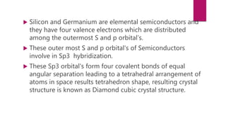
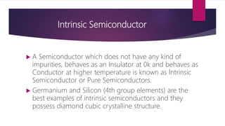
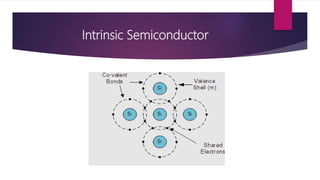
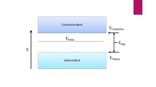
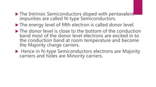
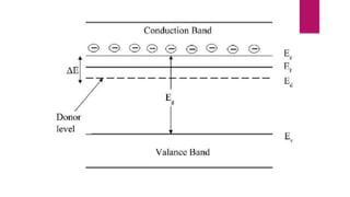
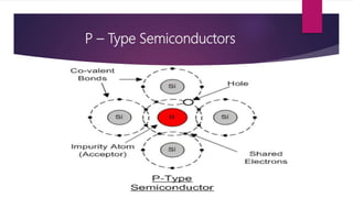
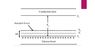
PONDICHERRY UNIVERSITY
DEPARTMENT OF ELECTRONICS AND
COMMUNICATION ENGINEERING
HIGH SPEED SEMICONDUCTOR DEVICES
TOPIC : SEMICONDUCTOR AND ITS TYPES
GUIDED BY : PROF.DR.K.ANUSUDHA PRESENTED BY : ARUNKUMAR G(21304004)
CONTENTS
 INTRODUCTION
 DEFINITION OF SEMICONDUCTOR
 TYPES OF SEMICONDUCTOR
 (a) INTRINSIC SEMICONDUCTOR
 (b) EXTRINSIC SEMICONDUCTOR
 CARRIER CONCENTRATION
 ENERGY BAND DIAGRAM
 ADVANTAGES
 DISADVANTAGES
 CONCLUSION
Introduction
 A semiconductor can be considered a material having
a conductivity ranging between that of an insulator
and a metal. A crucial property of semiconductors is
the band gap; a range of forbidden energies within
the electronic structure of the material.
Semiconductor
 Semiconductors are material whose electronic properties are
intermediate between those of Metals and Insulators.
 They have conductivities in the range of 10^-4to 10^+4 S/m.
 The interesting feature about semiconductors is that they are bipolar
and current is transported by two charge carriers of opposite sign.
 These intermediate properties are determined by
1.Crystal Structure bonding Characteristics.
2.Electronic Energy bands.
 Silicon and Germanium are elemental semiconductors and
they have four valence electrons which are distributed
among the outermost S and p orbital’s.
 These outer most S and p orbital's of Semiconductors
involve in Sp3 hybridization.
 These Sp3 orbital's form four covalent bonds of equal
angular separation leading to a tetrahedral arrangement of
atoms in space results tetrahedron shape, resulting crystal
structure is known as Diamond cubic crystal structure.
Types of semiconductor
 Semiconductors are mainly two types
1.Intrinsic (pure) Semiconductors
2.Extrinsic (Impure) Semiconductors
Intrinsic Semiconductor
 A Semiconductor which does not have any kind of
impurities, behaves as an Insulator at 0k and behaves as
Conductor at higher temperature is known as Intrinsic
Semiconductor or Pure Semiconductors.
 Germanium and Silicon (4th group elements) are the
best examples of intrinsic semiconductors and they
possess diamond cubic crystalline structure.
Intrinsic Semiconductor
Carrier Concentration in Intrinsic Semiconductor
 When a suitable form of Energy is supplied to a
Semiconductor then electrons take transition from Valence
band to Conduction band.
 Hence a free electron in Conduction band and
simultaneously free hole in Valence band is formed. This
phenomenon is known as Electron - Hole pair generation.
 In Intrinsic Semiconductor the Number of Conduction
electrons will be equal to the Number of Vacant sites or
holes in the valence band.
Extrinsic Semiconductors
 The Extrinsic Semiconductors are those in which impurities of
large quantity are present. Usually, the impurities can be
either 3rd group elements or 5th group elements.
 Based on the impurities present in the Extrinsic
Semiconductors, they are classified into two categories.
1. N-type semiconductors
2. P-type semiconductors
N – Type Semiconductors
 When any pentavalent element such as Phosphorous, Arsenic
or Antimony is added to the intrinsic Semiconductor, four
electrons are involved in covalent bonding with four
neighboring pure Semiconductor atoms.
 The fifth electron is weakly bound to the parent atom. And
even for lesser thermal energy it is released Leaving the parent
atom positively ionized.
N – Type Semiconductors
 The Intrinsic Semiconductors doped with pentavalent
impurities are called N-type Semiconductors.
 The energy level of fifth electron is called donor level.
 The donor level is close to the bottom of the conduction
band most of the donor level electrons are excited in to
the conduction band at room temperature and become
the Majority charge carriers.
 Hence in N-type Semiconductors electrons are Majority
carriers and holes are Minority carriers.
Carrier Concentration in N - Type Semiconductor
 Consider Nd is the donor Concentration i.e., the number of
donor atoms per unit volume of the material and Ed is the
donor energy level.
 At very low temperatures all donor levels are filled with
electrons.
 With increase of temperature more and more donor atoms
get ionized and the density of electrons in the conduction
band increases.
P – Type Semiconductors
 When a trivalent elements such as Al, Ga or Indium have three electrons in their
outer most orbits , added to the intrinsic semiconductor all the three electrons of
Indium are engaged in covalent bonding with the three neighboring Si atoms.
 Indium needs one more electron to complete its bond. this electron maybe
supplied by Silicon , there by creating a vacant electron site or hole on the
semiconductor atom.
 Indium accepts one extra electron, the energy level of this impurity atom is
called acceptor level and this acceptor level lies just above the valence band.
 These type of trivalent impurities are called acceptor impurities and the
semiconductors doped the acceptor impurities are called P-type semiconductors
P – Type Semiconductors
 Even at relatively low temperatures, these acceptor
atoms get ionized taking electrons from valence
band and thus giving rise to holes in valence band
for conduction.
 Due to ionization of acceptor atoms only holes and
no electrons are created.
 Thus holes are more in number than electrons and
hence holes are majority carriers and electros are
minority carriers in P-type semiconductors.
Carrier Concentration in P - Type Semiconductor
 The term p-type refers to the positive charge of a hole.
 As opposed to n-type semiconductors, p-type
semiconductors have a larger hole concentration than
electron concentration.
 In p-type semiconductors, holes are the majority carriers
and electrons are the minority carriers.
Advantages
 A semiconductor device on changing temperature can be
used as a conductor as well as an insulator.
 This is the main advantage of a semiconductor device.it is
also light weight, small, cheap and finds many applications
in modern devices like computers, electrical appliances.
Disadvantages
 The noise level is too much higher in semiconductor
devices as compared to the vacuum tubes.
 In when we have to use the ordinary semiconductor
devices cannot handle as more power as ordinary
vacuum tubes can do.
 In the high-frequency range, they have poor
performance.
Conclusion
The development of power semiconductor devices is
very essential for modern electronics. The power devices
based on new structures and materials are promising and
commercially realistic for future electronic developments.

Semiconductor and it's types

  • 1.
    PONDICHERRY UNIVERSITY DEPARTMENT OFELECTRONICS AND COMMUNICATION ENGINEERING HIGH SPEED SEMICONDUCTOR DEVICES TOPIC : SEMICONDUCTOR AND ITS TYPES GUIDED BY : PROF.DR.K.ANUSUDHA PRESENTED BY : ARUNKUMAR G(21304004)
  • 2.
    CONTENTS  INTRODUCTION  DEFINITIONOF SEMICONDUCTOR  TYPES OF SEMICONDUCTOR  (a) INTRINSIC SEMICONDUCTOR  (b) EXTRINSIC SEMICONDUCTOR  CARRIER CONCENTRATION  ENERGY BAND DIAGRAM  ADVANTAGES  DISADVANTAGES  CONCLUSION
  • 3.
    Introduction  A semiconductorcan be considered a material having a conductivity ranging between that of an insulator and a metal. A crucial property of semiconductors is the band gap; a range of forbidden energies within the electronic structure of the material.
  • 4.
    Semiconductor  Semiconductors arematerial whose electronic properties are intermediate between those of Metals and Insulators.  They have conductivities in the range of 10^-4to 10^+4 S/m.  The interesting feature about semiconductors is that they are bipolar and current is transported by two charge carriers of opposite sign.  These intermediate properties are determined by 1.Crystal Structure bonding Characteristics. 2.Electronic Energy bands.
  • 5.
     Silicon andGermanium are elemental semiconductors and they have four valence electrons which are distributed among the outermost S and p orbital’s.  These outer most S and p orbital's of Semiconductors involve in Sp3 hybridization.  These Sp3 orbital's form four covalent bonds of equal angular separation leading to a tetrahedral arrangement of atoms in space results tetrahedron shape, resulting crystal structure is known as Diamond cubic crystal structure.
  • 6.
    Types of semiconductor Semiconductors are mainly two types 1.Intrinsic (pure) Semiconductors 2.Extrinsic (Impure) Semiconductors
  • 7.
    Intrinsic Semiconductor  ASemiconductor which does not have any kind of impurities, behaves as an Insulator at 0k and behaves as Conductor at higher temperature is known as Intrinsic Semiconductor or Pure Semiconductors.  Germanium and Silicon (4th group elements) are the best examples of intrinsic semiconductors and they possess diamond cubic crystalline structure.
  • 8.
  • 10.
    Carrier Concentration inIntrinsic Semiconductor  When a suitable form of Energy is supplied to a Semiconductor then electrons take transition from Valence band to Conduction band.  Hence a free electron in Conduction band and simultaneously free hole in Valence band is formed. This phenomenon is known as Electron - Hole pair generation.  In Intrinsic Semiconductor the Number of Conduction electrons will be equal to the Number of Vacant sites or holes in the valence band.
  • 11.
    Extrinsic Semiconductors  TheExtrinsic Semiconductors are those in which impurities of large quantity are present. Usually, the impurities can be either 3rd group elements or 5th group elements.  Based on the impurities present in the Extrinsic Semiconductors, they are classified into two categories. 1. N-type semiconductors 2. P-type semiconductors
  • 12.
    N – TypeSemiconductors  When any pentavalent element such as Phosphorous, Arsenic or Antimony is added to the intrinsic Semiconductor, four electrons are involved in covalent bonding with four neighboring pure Semiconductor atoms.  The fifth electron is weakly bound to the parent atom. And even for lesser thermal energy it is released Leaving the parent atom positively ionized.
  • 13.
    N – TypeSemiconductors
  • 14.
     The IntrinsicSemiconductors doped with pentavalent impurities are called N-type Semiconductors.  The energy level of fifth electron is called donor level.  The donor level is close to the bottom of the conduction band most of the donor level electrons are excited in to the conduction band at room temperature and become the Majority charge carriers.  Hence in N-type Semiconductors electrons are Majority carriers and holes are Minority carriers.
  • 16.
    Carrier Concentration inN - Type Semiconductor  Consider Nd is the donor Concentration i.e., the number of donor atoms per unit volume of the material and Ed is the donor energy level.  At very low temperatures all donor levels are filled with electrons.  With increase of temperature more and more donor atoms get ionized and the density of electrons in the conduction band increases.
  • 17.
    P – TypeSemiconductors  When a trivalent elements such as Al, Ga or Indium have three electrons in their outer most orbits , added to the intrinsic semiconductor all the three electrons of Indium are engaged in covalent bonding with the three neighboring Si atoms.  Indium needs one more electron to complete its bond. this electron maybe supplied by Silicon , there by creating a vacant electron site or hole on the semiconductor atom.  Indium accepts one extra electron, the energy level of this impurity atom is called acceptor level and this acceptor level lies just above the valence band.  These type of trivalent impurities are called acceptor impurities and the semiconductors doped the acceptor impurities are called P-type semiconductors
  • 18.
    P – TypeSemiconductors
  • 20.
     Even atrelatively low temperatures, these acceptor atoms get ionized taking electrons from valence band and thus giving rise to holes in valence band for conduction.  Due to ionization of acceptor atoms only holes and no electrons are created.  Thus holes are more in number than electrons and hence holes are majority carriers and electros are minority carriers in P-type semiconductors.
  • 21.
    Carrier Concentration inP - Type Semiconductor  The term p-type refers to the positive charge of a hole.  As opposed to n-type semiconductors, p-type semiconductors have a larger hole concentration than electron concentration.  In p-type semiconductors, holes are the majority carriers and electrons are the minority carriers.
  • 22.
    Advantages  A semiconductordevice on changing temperature can be used as a conductor as well as an insulator.  This is the main advantage of a semiconductor device.it is also light weight, small, cheap and finds many applications in modern devices like computers, electrical appliances.
  • 23.
    Disadvantages  The noiselevel is too much higher in semiconductor devices as compared to the vacuum tubes.  In when we have to use the ordinary semiconductor devices cannot handle as more power as ordinary vacuum tubes can do.  In the high-frequency range, they have poor performance.
  • 24.
    Conclusion The development ofpower semiconductor devices is very essential for modern electronics. The power devices based on new structures and materials are promising and commercially realistic for future electronic developments.