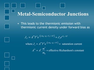
Majority Carrier
Diode


       By Dr. Ghanshyam Singh
Junction Breakdown
• When a huge reverse voltage is applied to a p-n
  junction, the junction breaks down and conducts
  a very large current.
• Although, the breakdown process is not
  naturally destructive, the maximum current mus
  t be limited by an external circuit to avoid exces
  sive junction heating.
• There are mechanisms dealing with the
  breakdown: zener diode, tunneling diode and av
  alanche diode.
Tunneling Effect
                   • If a very high electric
                     field is applied to a p-n
                     junction in the reverse
                     direction, a valence
                     electron can make a
                     transition from the
                     valence band to the
                     conduction band by
                     penetrating through the
                     energy bandgap called
                     tunneling.
                   • The typical field for Si
                     and GaAs is about 106
                     V/cm or higher.
Tunneling Effect
• To achieve such a high field, the doping
  concentration for both p- and n-regions must be
  very high such as more than 5 x 1017 cm-3.
• The breakdown voltage for Si and GaAs
  junctions about 4Eg/e is the result of the tunneli
  ng effect. With the breakdown voltage is more t
  han 6Eg/e, the breakdown mechanism is the resu
  lt of avalanche multiplication.
• As the voltage is in between 4Eg/e and 6Eg/e, the
  breakdown is due to a mix of both tunneling
  effect and avalanche multiplication.
Backward Diode
• a backward diode (also called back diode) is a
  variation on a Zener diode or tunnel diode having a
  better conduction for small reverse biases (for example
  –0.1 to –0.6 V) than for forward bias voltages.

• The schematic symbol for the backward diode,
  annotated to show which side is P type and which is N;
  current flows most easily from N to P, backward
  relative to the arrow.
Current–voltage characteristics
• The forward I–V characteristic is the same as that of an
  ordinary P–N diode.
• The breakdown starts when reverse voltage is applied. In
  the case of Zener breakdown, it starts at a particular
  voltage. In this diode the voltage remains relatively
  constant (independent of current) when it is connected in
  reverse bias.
• The backward diode is a special form of tunnel diode in
  which the tunneling phenomenon is only incipient, and
  the negative resistance region virtually disappears. The
  forward current is very small and becomes equivalent to
  the reverse current of a conventional diode.
Energy Band diagram


Electron energy is on the vertical axis, position within the
device is on the horizontal axis. The backward diode has the
unusual property that the so-called reverse bias direction
actually has more current flow than the so-called forward
bias.
Applications of backward diodes
• Detector
  Since it has low capacitance and no charge storage
  effect, and a strongly nonlinear small-signal
  characteristic, the backward diode can be used as a
  detector up to 40 GHz.
• Rectifier
  A backward diode can be used for rectifying weak signals
  with peak amplitudes of 0.1 to 0.7 V.
• Switch
  Backward diode can be used in high speed switching
  applications.
Schottky diode
• The Schottky diode also known as hot carrier
  diode is a semiconductor diode with a low
  forward voltage drop and a very fast switching
  action.
• When current flows through a diode there is a
  small voltage drop across the diode terminals.
  A normal silicon diode has a voltage drop
  between 0.6–1.7 volts, while a Schottky diode
  voltage drop is between approximately 0.15–
  0.45 volts. This lower voltage drop can provide
  higher switching speed and better system
  efficiency.
Schottky effect
• In electron emission devices, especially electron guns, the
  thermionic electron emitter will be biased negative relative
  to its surroundings. This creates an electric field of
  magnitude F at the emitter surface. Without the field, the
  surface barrier seen by an escaping Fermi-level electron has
  height W equal to the local work-function. The electric field
  lowers the surface barrier by an amount ΔW, and increases
  the emission current. This is known as the Schottky
  effect or field enhanced thermionic emission. It can be
  modeled by a simple modification of the Richardson
  equation, by replacing W by (W − ΔW). This gives the
  equation
Applications
Voltage clamping
• While standard silicon diodes have a forward voltage drop
  of about 0.7 volts and germanium diodes 0.3 volts,
  Schottky diodes’ voltage drop at forward biases of around
  1 mA is in the range 0.15 V to 0.46 V which makes them
  useful in voltage clamping applications and prevention
  of transistor saturation. This is due to the higher current
  density in the Schottky diode.
Reverse current and discharge protection
• Because of a Schottky diode's low forward voltage drop,
  less energy is wasted as heat making them the most
  efficient choice for applications sensitive to efficiency.
Power supply
• Schottky diodes can be used in power supply circuits in
  products that have both an internal battery and a mains
  adapter input, or similar.
Heterojunction
                 A heterojunction is
                 defined as a junction
                 formed by two semicondu
                 ctors with different energ
                 y bandgaps Eg, different di
                 electric permittivities εs,
                 different work function e
                 φs, and different electron
                 affinities eχ.
Heterojunction
             • The difference energy
               between two conduction band
               edges and between two valen
               ce band edges are represente
               d by ∆EC and ∆EV, respectively
               , as
                           ∆EC = e ( χ 2 − χ1 )

             ∆EV = Eg1 + eχ1 − ( E g 2 + eχ 2 ) = ∆E g − ∆EC


                 where ∆Eg is the difference
                 energy bandgap of two
                 semiconductors.
Heterojunction
• Generally, heterojunction has to be formed
  between semiconductors with closely matched
  lattice constants.
• For example, the AlxGa1-xAs material is the most
  important material for heterojunction.
• When x = 0, the bandgap of GaAs is 1.42 eV with
  a lattice constant of 5.6533 Å at 300 K.
• When x = 1, the bandgap of AlAs is 2.17 eV with
  a lattice constant of 5.6605 Å.
Heterojunction
• We clearly see that the lattice constant is
  almost constant as x increased. The total built-
  in potential Vbi can be expressed by
                     Vbi = Vb1 + Vb 2
                       ε 2 N 2 ( Vbi − V )
                 Vb1 =
                        ε1 N1 + ε 2 N 2
                        ε1 N1 ( Vbi − V )
                 Vb 2 =
                         ε1 N1 + ε 2 N 2

where N1 and N2 are the doping concentrations in
  semiconductor 1 and 2, respectively.
Heterojunction
• The depletion widths x1 and x2 can be found by


                    2ε1ε 2 N 2 ( Vbi − V )
             x1 =
                    eN1 ( ε1 N1 + ε 2 N 2 )
                     2ε1ε 2 N1 ( Vbi − V )
             x2 =
                    eN 2 ( ε1 N1 + ε 2 N 2 )
Heterojunction
Ex. Consider an ideal abrupt heterojunction with a
  built-in potential of 1.6 V. The impurity concent
  rations in semiconductor 1 and 2 are 1 x 10¹⁶ don
  ors/cm3 and 3 x 10¹⁹ acceptors/cm3, and the diele
  ctric constants are 12 and 13, respectively. Find
  the electrostatic potential and depletion width i
  n each material at thermal equilibrium.
Heterojunction
                     13 × ( 3 × 10¹⁹ ) × 1.6
Soln   Vb1 =
               12 × ( 1 × 10
                                                     = 1.6 V
                           16
                              ) + 13 × ( 3 ×10 )19


                      12 × ( 1× 10 ) × 1.6
                                    16
                                                                −4
       Vb 2  =                                   = 4.9 × 10 V
               12 × ( 1 × 10 ) + 13 × ( 3 × 10 )
                               16               19


                   2 × 12 × 13 × ( 8.85 × 10 ) × 3 × 10 × 1.6
                                               −14         19
                                                                          −5
       x1   =                                                 = 4.608 × 10        cm
               1.6 × 10 × 1× 10 × ( 12 × 10 + 13 × 3 × 10 )
                         −19             16          16              19


                   2 × 12 × 13 × ( 8.85 × 10 ) × 1× 10 × 1.6
                                               −14         16
                                                                             −8
       x2   =                                                 = 1.536 × 10        cm
                1.6 × 10 × 3 × 10 × ( 12 × 10 + 13 × 3 × 10 )
                         −19             19          16              19


Note: Most of the built-in potential is in the
semiconductor with a lower doping concentration and
also its depletion width is much wider.
Metal-Semiconductor Junctions


• The MS junction is more
  likely known as the Schott
  ky-barrier diode.
• Let’s consider metal band
  and semiconductor band
  diagram before the contac
  t.
Metal-Semiconductor Junctions
               • When the metal and
                 semiconductor are joined,
                 electrons from the semico
                 nductor cross over to the
                 metal until the Fermi leve
                 l is aligned (Thermal equil
                 ibrium condition).
               • This leaves ionized donors
                 as fixed positive charges
                 that produce an internal e
                 lectric field as the case of
                 one-sided p-n junction.
Metal-Semiconductor Junctions


• At equilibrium, equal number of electrons across the
  interface in opposite directions.
• Hence, no net transport of charge, electron current Ie
  equals to zero. The built-in voltage Vbi = φm - φs.
• The barrier for electrons to flow from the metal to
  semiconductor is given by eφb = e(φm - χs) or it is called the
  barrier height of MS contact.
Metal-Semiconductor Junctions
• When a voltage is applied, the barrier height
  remains fixed but the built-in voltage changes as
  increasing when reverse biased and decreasing
  when forward biased.
Metal-Semiconductor Junctions
• Reverse bias


• Few electrons move across the interface from metal to
  semiconductor due to a barrier, but it is harder for elect
  rons in the semiconductor to move to the metal.
• Hence, net electron transport is caused by electrons
  moving from metal to semiconductor. Electron current fl
  ows from right to left which is a small value.
Metal-Semiconductor Junctions
• Forward bias


• Few electrons move across the interface from metal to
  semiconductor, but many electrons move across the inter
  face from semiconductor to metal due to the reduced bar
  rier.
• Therefore, net transport of charge flows from
  semiconductor to metal and electron current flows from l
  eft to right.
Metal-Semiconductor Junctions
• Under forward bias, the electrons emitted to
  the metal have greater energy than that of the
  metal electrons by about e(φm - χs).
• These electrons are called hot-carrier since
  their equivalent temperature is higher than that
  of electrons in the metal.
• Therefore, sometimes, Schottky-diode is called
  “hot-carrier diode”.
Metal-Semiconductor Junctions
• This leads to the thermionic emission with
  thermionic current density under forward bias as

                     − e( φm − χ s −VF ) / kT 
     J F = A**T 2e                            
                                                   = J s e eVF / kT
                                 − e( φm − χ s ) / kT 
     where J s = A**T 2e                              
                                                           = saturation current
                 m*
           A =A.
             **
                    = effective Richardson's constant
                       *

                 m0
Metal-Semiconductor Junctions
• This behavior is referred to a rectification and
  can be described by an ideal diode equation of

                J = J s ( eeV / kT − 1)

  where V positive for forward bias and negative
  for reverse bias.
Metal-Semiconductor Junctions
• The space-charge region width of Schottky diode is
  identical to that of a one-sided p-n junction.
• Therefore, under reverse bias, they can contain the
  charges in their depletion region and this is called Schott
  ky diode capacitance.
Metal-Semiconductor Junctions
Ex. A Schottky junction is formed between Au and
  n-type semiconductor of ND = 1016 cm-3. Area of ju
  nction = 10-3 cm2 and me*= 0.92 m0. Work function
  of gold is 4.77 eV and eχs = 4.05 eV. Find current
  at VF = 0.3 volts.
Metal-Semiconductor Junctions
Soln
                 *
                me
       A** = A*    = 120 × 0.92 = 110 A/ ( cm 2 .K )
                m0
                       − e( φm − χ s ) / kT
       J s = A**T 2e
       J = J s ( eeV / kT − 1)

         = ( 110 × 3002 ) × e      {     − ( 4.77 − 4.05) / 0.0259 
                                                                   
                                                                        }   . ( e0.3 / 0.0259 − 1)

         = 0.897 A/(cm 2 )
       I = A × J = ( 10−3 ) ( 0.897 ) = 0.897 mA
Metal-Semiconductor Junctions
Ex. Si-Schottky diode of 100 μm diameter has (1/
  C2) v.s. VR slope of 3 x 10¹⁹ F-2V-1. Given εr = 11.9 fo
  r Si. Find NB for this semiconductor.
Metal-Semiconductor Junctions
Soln
       1 2 ( Vbi + VR )                  C
          =             ;        Cj =        [F/cm 2 ]
        2
       Cj    eε s N B                   Area
                    2
       slope =            [cm 4 F-2 V -1 ]
                 eε s N B
                       2
       NB =
              slope × Area 2 × eε s
                                                2
       NB =
                                    −4 2 
                                             2
                                                                          
                    19    100 × 10                                   
              3 × 10 π                              −19         −12
                                        ÷  × 1.6 × 10 × 8.85 × 10 × 11.9 
                              2       
                                                                       
          = 6.414 × 1019 cm -3
Ohmic contact
• This contact is defined as a junction that will
  not add a significant parasitic impedance to the
  structure on which it is used and will not
  sufficiently change the equilibrium-carrier
  densities within the semiconductor to affect the
  device characteristics.
• The I-V characteristic of ohmic contact is linear
  for an ideal case.
Ohmic contact
• A specific contact resistance RC is given by


                1   ∂J                      −1
                  =             Ω.cm 2 
                                       
                RC ∂V    V =0


• A good ohmic contact should have a small
  specific contact resistance about 10-6 Ω.cm2.
Ohmic contact
                • When the semiconductor
                  is heavily doped with an
                  impurity density of 1019 c
                  m-3 or higher, the depleti
                  on layer of the junction
                  becomes very thin so tha
                  t carriers can tunnel inst
                  ead of going over the pot
                  ential barrier.
THANK YOU

Majority carrier diode

  • 1.
    Majority Carrier Diode By Dr. Ghanshyam Singh
  • 2.
    Junction Breakdown • Whena huge reverse voltage is applied to a p-n junction, the junction breaks down and conducts a very large current. • Although, the breakdown process is not naturally destructive, the maximum current mus t be limited by an external circuit to avoid exces sive junction heating. • There are mechanisms dealing with the breakdown: zener diode, tunneling diode and av alanche diode.
  • 3.
    Tunneling Effect • If a very high electric field is applied to a p-n junction in the reverse direction, a valence electron can make a transition from the valence band to the conduction band by penetrating through the energy bandgap called tunneling. • The typical field for Si and GaAs is about 106 V/cm or higher.
  • 4.
    Tunneling Effect • Toachieve such a high field, the doping concentration for both p- and n-regions must be very high such as more than 5 x 1017 cm-3. • The breakdown voltage for Si and GaAs junctions about 4Eg/e is the result of the tunneli ng effect. With the breakdown voltage is more t han 6Eg/e, the breakdown mechanism is the resu lt of avalanche multiplication. • As the voltage is in between 4Eg/e and 6Eg/e, the breakdown is due to a mix of both tunneling effect and avalanche multiplication.
  • 5.
    Backward Diode • abackward diode (also called back diode) is a variation on a Zener diode or tunnel diode having a better conduction for small reverse biases (for example –0.1 to –0.6 V) than for forward bias voltages. • The schematic symbol for the backward diode, annotated to show which side is P type and which is N; current flows most easily from N to P, backward relative to the arrow.
  • 6.
    Current–voltage characteristics • Theforward I–V characteristic is the same as that of an ordinary P–N diode. • The breakdown starts when reverse voltage is applied. In the case of Zener breakdown, it starts at a particular voltage. In this diode the voltage remains relatively constant (independent of current) when it is connected in reverse bias. • The backward diode is a special form of tunnel diode in which the tunneling phenomenon is only incipient, and the negative resistance region virtually disappears. The forward current is very small and becomes equivalent to the reverse current of a conventional diode.
  • 7.
    Energy Band diagram Electronenergy is on the vertical axis, position within the device is on the horizontal axis. The backward diode has the unusual property that the so-called reverse bias direction actually has more current flow than the so-called forward bias.
  • 8.
    Applications of backwarddiodes • Detector Since it has low capacitance and no charge storage effect, and a strongly nonlinear small-signal characteristic, the backward diode can be used as a detector up to 40 GHz. • Rectifier A backward diode can be used for rectifying weak signals with peak amplitudes of 0.1 to 0.7 V. • Switch Backward diode can be used in high speed switching applications.
  • 9.
    Schottky diode • The Schottkydiode also known as hot carrier diode is a semiconductor diode with a low forward voltage drop and a very fast switching action. • When current flows through a diode there is a small voltage drop across the diode terminals. A normal silicon diode has a voltage drop between 0.6–1.7 volts, while a Schottky diode voltage drop is between approximately 0.15– 0.45 volts. This lower voltage drop can provide higher switching speed and better system efficiency.
  • 10.
    Schottky effect • Inelectron emission devices, especially electron guns, the thermionic electron emitter will be biased negative relative to its surroundings. This creates an electric field of magnitude F at the emitter surface. Without the field, the surface barrier seen by an escaping Fermi-level electron has height W equal to the local work-function. The electric field lowers the surface barrier by an amount ΔW, and increases the emission current. This is known as the Schottky effect or field enhanced thermionic emission. It can be modeled by a simple modification of the Richardson equation, by replacing W by (W − ΔW). This gives the equation
  • 11.
    Applications Voltage clamping • Whilestandard silicon diodes have a forward voltage drop of about 0.7 volts and germanium diodes 0.3 volts, Schottky diodes’ voltage drop at forward biases of around 1 mA is in the range 0.15 V to 0.46 V which makes them useful in voltage clamping applications and prevention of transistor saturation. This is due to the higher current density in the Schottky diode. Reverse current and discharge protection • Because of a Schottky diode's low forward voltage drop, less energy is wasted as heat making them the most efficient choice for applications sensitive to efficiency. Power supply • Schottky diodes can be used in power supply circuits in products that have both an internal battery and a mains adapter input, or similar.
  • 12.
    Heterojunction A heterojunction is defined as a junction formed by two semicondu ctors with different energ y bandgaps Eg, different di electric permittivities εs, different work function e φs, and different electron affinities eχ.
  • 13.
    Heterojunction • The difference energy between two conduction band edges and between two valen ce band edges are represente d by ∆EC and ∆EV, respectively , as ∆EC = e ( χ 2 − χ1 ) ∆EV = Eg1 + eχ1 − ( E g 2 + eχ 2 ) = ∆E g − ∆EC where ∆Eg is the difference energy bandgap of two semiconductors.
  • 14.
    Heterojunction • Generally, heterojunctionhas to be formed between semiconductors with closely matched lattice constants. • For example, the AlxGa1-xAs material is the most important material for heterojunction. • When x = 0, the bandgap of GaAs is 1.42 eV with a lattice constant of 5.6533 Å at 300 K. • When x = 1, the bandgap of AlAs is 2.17 eV with a lattice constant of 5.6605 Å.
  • 15.
    Heterojunction • We clearlysee that the lattice constant is almost constant as x increased. The total built- in potential Vbi can be expressed by Vbi = Vb1 + Vb 2 ε 2 N 2 ( Vbi − V ) Vb1 = ε1 N1 + ε 2 N 2 ε1 N1 ( Vbi − V ) Vb 2 = ε1 N1 + ε 2 N 2 where N1 and N2 are the doping concentrations in semiconductor 1 and 2, respectively.
  • 16.
    Heterojunction • The depletionwidths x1 and x2 can be found by 2ε1ε 2 N 2 ( Vbi − V ) x1 = eN1 ( ε1 N1 + ε 2 N 2 ) 2ε1ε 2 N1 ( Vbi − V ) x2 = eN 2 ( ε1 N1 + ε 2 N 2 )
  • 17.
    Heterojunction Ex. Consider anideal abrupt heterojunction with a built-in potential of 1.6 V. The impurity concent rations in semiconductor 1 and 2 are 1 x 10¹⁶ don ors/cm3 and 3 x 10¹⁹ acceptors/cm3, and the diele ctric constants are 12 and 13, respectively. Find the electrostatic potential and depletion width i n each material at thermal equilibrium.
  • 18.
    Heterojunction 13 × ( 3 × 10¹⁹ ) × 1.6 Soln Vb1 = 12 × ( 1 × 10 = 1.6 V 16 ) + 13 × ( 3 ×10 )19 12 × ( 1× 10 ) × 1.6 16 −4 Vb 2 = = 4.9 × 10 V 12 × ( 1 × 10 ) + 13 × ( 3 × 10 ) 16 19 2 × 12 × 13 × ( 8.85 × 10 ) × 3 × 10 × 1.6 −14 19 −5 x1 = = 4.608 × 10 cm 1.6 × 10 × 1× 10 × ( 12 × 10 + 13 × 3 × 10 ) −19 16 16 19 2 × 12 × 13 × ( 8.85 × 10 ) × 1× 10 × 1.6 −14 16 −8 x2 = = 1.536 × 10 cm 1.6 × 10 × 3 × 10 × ( 12 × 10 + 13 × 3 × 10 ) −19 19 16 19 Note: Most of the built-in potential is in the semiconductor with a lower doping concentration and also its depletion width is much wider.
  • 19.
    Metal-Semiconductor Junctions • TheMS junction is more likely known as the Schott ky-barrier diode. • Let’s consider metal band and semiconductor band diagram before the contac t.
  • 20.
    Metal-Semiconductor Junctions • When the metal and semiconductor are joined, electrons from the semico nductor cross over to the metal until the Fermi leve l is aligned (Thermal equil ibrium condition). • This leaves ionized donors as fixed positive charges that produce an internal e lectric field as the case of one-sided p-n junction.
  • 21.
    Metal-Semiconductor Junctions • Atequilibrium, equal number of electrons across the interface in opposite directions. • Hence, no net transport of charge, electron current Ie equals to zero. The built-in voltage Vbi = φm - φs. • The barrier for electrons to flow from the metal to semiconductor is given by eφb = e(φm - χs) or it is called the barrier height of MS contact.
  • 22.
    Metal-Semiconductor Junctions • Whena voltage is applied, the barrier height remains fixed but the built-in voltage changes as increasing when reverse biased and decreasing when forward biased.
  • 23.
    Metal-Semiconductor Junctions • Reversebias • Few electrons move across the interface from metal to semiconductor due to a barrier, but it is harder for elect rons in the semiconductor to move to the metal. • Hence, net electron transport is caused by electrons moving from metal to semiconductor. Electron current fl ows from right to left which is a small value.
  • 24.
    Metal-Semiconductor Junctions • Forwardbias • Few electrons move across the interface from metal to semiconductor, but many electrons move across the inter face from semiconductor to metal due to the reduced bar rier. • Therefore, net transport of charge flows from semiconductor to metal and electron current flows from l eft to right.
  • 25.
    Metal-Semiconductor Junctions • Underforward bias, the electrons emitted to the metal have greater energy than that of the metal electrons by about e(φm - χs). • These electrons are called hot-carrier since their equivalent temperature is higher than that of electrons in the metal. • Therefore, sometimes, Schottky-diode is called “hot-carrier diode”.
  • 26.
    Metal-Semiconductor Junctions • Thisleads to the thermionic emission with thermionic current density under forward bias as − e( φm − χ s −VF ) / kT  J F = A**T 2e   = J s e eVF / kT − e( φm − χ s ) / kT  where J s = A**T 2e   = saturation current m* A =A. ** = effective Richardson's constant * m0
  • 27.
    Metal-Semiconductor Junctions • Thisbehavior is referred to a rectification and can be described by an ideal diode equation of J = J s ( eeV / kT − 1) where V positive for forward bias and negative for reverse bias.
  • 28.
    Metal-Semiconductor Junctions • Thespace-charge region width of Schottky diode is identical to that of a one-sided p-n junction. • Therefore, under reverse bias, they can contain the charges in their depletion region and this is called Schott ky diode capacitance.
  • 29.
    Metal-Semiconductor Junctions Ex. ASchottky junction is formed between Au and n-type semiconductor of ND = 1016 cm-3. Area of ju nction = 10-3 cm2 and me*= 0.92 m0. Work function of gold is 4.77 eV and eχs = 4.05 eV. Find current at VF = 0.3 volts.
  • 30.
    Metal-Semiconductor Junctions Soln * me A** = A* = 120 × 0.92 = 110 A/ ( cm 2 .K ) m0 − e( φm − χ s ) / kT J s = A**T 2e J = J s ( eeV / kT − 1) = ( 110 × 3002 ) × e { − ( 4.77 − 4.05) / 0.0259    } . ( e0.3 / 0.0259 − 1) = 0.897 A/(cm 2 ) I = A × J = ( 10−3 ) ( 0.897 ) = 0.897 mA
  • 31.
    Metal-Semiconductor Junctions Ex. Si-Schottkydiode of 100 μm diameter has (1/ C2) v.s. VR slope of 3 x 10¹⁹ F-2V-1. Given εr = 11.9 fo r Si. Find NB for this semiconductor.
  • 32.
    Metal-Semiconductor Junctions Soln 1 2 ( Vbi + VR ) C = ; Cj = [F/cm 2 ] 2 Cj eε s N B Area 2 slope = [cm 4 F-2 V -1 ] eε s N B 2 NB = slope × Area 2 × eε s 2 NB =  −4 2  2  19    100 × 10    3 × 10 π  −19 −12 ÷  × 1.6 × 10 × 8.85 × 10 × 11.9    2       = 6.414 × 1019 cm -3
  • 33.
    Ohmic contact • Thiscontact is defined as a junction that will not add a significant parasitic impedance to the structure on which it is used and will not sufficiently change the equilibrium-carrier densities within the semiconductor to affect the device characteristics. • The I-V characteristic of ohmic contact is linear for an ideal case.
  • 34.
    Ohmic contact • Aspecific contact resistance RC is given by 1 ∂J −1 = Ω.cm 2    RC ∂V V =0 • A good ohmic contact should have a small specific contact resistance about 10-6 Ω.cm2.
  • 35.
    Ohmic contact • When the semiconductor is heavily doped with an impurity density of 1019 c m-3 or higher, the depleti on layer of the junction becomes very thin so tha t carriers can tunnel inst ead of going over the pot ential barrier.
  • 36.