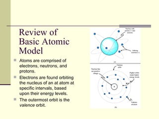
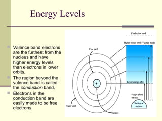
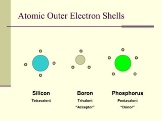
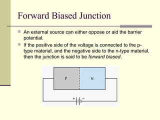
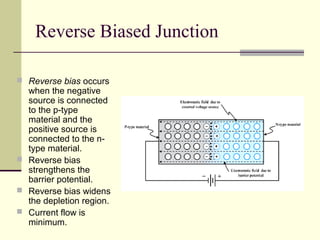
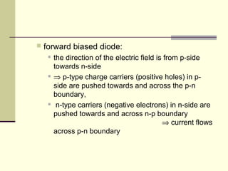
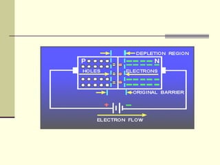
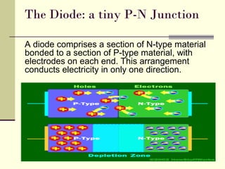
Semi-conductor Material
Presenter : Damion Lawrence
Review of
Basic Atomic
Model
 Atoms are comprised of
electrons, neutrons, and
protons.
 Electrons are found orbiting
the nucleus of an at atom at
specific intervals, based
upon their energy levels.
 The outermost orbit is the
valence orbit.
Energy Levels
 Valence band electrons
are the furthest from the
nucleus and have
higher energy levels
than electrons in lower
orbits.
 The region beyond the
valence band is called
the conduction band.
 Electrons in the
conduction band are
easily made to be free
electrons.
Intrinsic Semiconductors
 Silicon, germanium, and gallium arsenide are
the primary materials used in semiconductor
devices.
 Silicon and germanium are elements and are
intrinsic semiconductors.
 In pure form, silicon and germanium do not
exhibit the characteristics needed for practical
solid-state devices.
Semiconductor Crystals
 Tetravalent atoms such as silicon, gallium
arsenide, and germanium bond together to
form a crystal or crystal lattice.
 Because of the crystalline structure of
semiconductor materials, valence electrons
are shared between atoms.
 This sharing of valence electrons is called
covalent bonding. Covalent bonding makes it
more difficult for materials to move their
electrons into the conduction band.
Electron Distribution
 As more energy is applied to a
semiconductor, more electrons will move into
the conduction band and current will flow
more easily through the material.
 Therefore, the resistance of intrinsic
semiconductor materials decreases with
increasing temperature.
 This is a negative temperature coefficient.
Semiconductor Doping
 Impurities are added to intrinsic
semiconductor materials to improve the
electrical properties of the material.
 This process is referred to as doping and the
resulting material is called extrinsic
semiconductor.
 There are two major classifications of doping
materials.
 Trivalent - aluminum, gallium, boron
 Pentavalent - antimony, arsenic, phosphorous
Atomic Outer Electron Shells
Silicon
Tetravalent
Boron
Trivalent
“Acceptor”
Phosphorus
Pentavalent
“Donor”
Forward Biased Junction
 An external source can either oppose or aid the barrier
potential.
 If the positive side of the voltage is connected to the p-
type material, and the negative side to the n-type material,
then the junction is said to be forward biased.
Forward Biased Junction
 In a forward biased junction, the following
conditions exist:
 Forward bias overcomes barrier potential.
 Forward bias narrows the depletion region.
 There is maximum current flow with forward
bias.
Reverse Biased Junction
 Reverse bias occurs
when the negative
source is connected
to the p-type
material and the
positive source is
connected to the n-
type material.
 Reverse bias
strengthens the
barrier potential.
 Reverse bias widens
the depletion region.
 Current flow is
minimum.
Reverse Biased Junction
 A reversed biased junction has zero current
flow (ideally).
 Reverse current is temperature dependent.
 If reverse biased is increased enough, the
reverse current increases dramatically.
 This breakdown is called junction breakdown.
The voltage required to reach this point is the
reverse breakdown voltage.
 As the breakdown occurs, avalanche may
occur and destroy the device if uncontrolled.
DIODE
 diode = “biased p-n junction”, i.e. p-n junction
with voltage applied across it
 “forward biased”: p-side more positive than n-
side;
 “reverse biased”: n-side more positive than p-
side;
 forward biased diode:
 the direction of the electric field is from p-side
towards n-side
 ⇒ p-type charge carriers (positive holes) in p-
side are pushed towards and across the p-n
boundary,
 n-type carriers (negative electrons) in n-side are
pushed towards and across n-p boundary
⇒ current flows
across p-n boundary
The Diode: a tiny P-N Junction
A diode comprises a section of N-type material
bonded to a section of P-type material, with
electrodes on each end. This arrangement
conducts electricity in only one direction.
 When no voltage is applied, to the diode,
electrons from the N-type material fill
holes from the P-type material along the
junction between the layers, forming a
depletion zone. In a depletion zone, the
semiconductor material is returned to its
original insulating state -- all of the holes are
filled, so there are no free electrons or empty
spaces for electrons, and charge can't flow.

Presentation on semiconductor

  • 1.
  • 2.
    Review of Basic Atomic Model Atoms are comprised of electrons, neutrons, and protons.  Electrons are found orbiting the nucleus of an at atom at specific intervals, based upon their energy levels.  The outermost orbit is the valence orbit.
  • 3.
    Energy Levels  Valenceband electrons are the furthest from the nucleus and have higher energy levels than electrons in lower orbits.  The region beyond the valence band is called the conduction band.  Electrons in the conduction band are easily made to be free electrons.
  • 4.
    Intrinsic Semiconductors  Silicon,germanium, and gallium arsenide are the primary materials used in semiconductor devices.  Silicon and germanium are elements and are intrinsic semiconductors.  In pure form, silicon and germanium do not exhibit the characteristics needed for practical solid-state devices.
  • 5.
    Semiconductor Crystals  Tetravalentatoms such as silicon, gallium arsenide, and germanium bond together to form a crystal or crystal lattice.  Because of the crystalline structure of semiconductor materials, valence electrons are shared between atoms.  This sharing of valence electrons is called covalent bonding. Covalent bonding makes it more difficult for materials to move their electrons into the conduction band.
  • 6.
    Electron Distribution  Asmore energy is applied to a semiconductor, more electrons will move into the conduction band and current will flow more easily through the material.  Therefore, the resistance of intrinsic semiconductor materials decreases with increasing temperature.  This is a negative temperature coefficient.
  • 7.
    Semiconductor Doping  Impuritiesare added to intrinsic semiconductor materials to improve the electrical properties of the material.  This process is referred to as doping and the resulting material is called extrinsic semiconductor.  There are two major classifications of doping materials.  Trivalent - aluminum, gallium, boron  Pentavalent - antimony, arsenic, phosphorous
  • 8.
    Atomic Outer ElectronShells Silicon Tetravalent Boron Trivalent “Acceptor” Phosphorus Pentavalent “Donor”
  • 9.
    Forward Biased Junction An external source can either oppose or aid the barrier potential.  If the positive side of the voltage is connected to the p- type material, and the negative side to the n-type material, then the junction is said to be forward biased.
  • 10.
    Forward Biased Junction In a forward biased junction, the following conditions exist:  Forward bias overcomes barrier potential.  Forward bias narrows the depletion region.  There is maximum current flow with forward bias.
  • 11.
    Reverse Biased Junction Reverse bias occurs when the negative source is connected to the p-type material and the positive source is connected to the n- type material.  Reverse bias strengthens the barrier potential.  Reverse bias widens the depletion region.  Current flow is minimum.
  • 12.
    Reverse Biased Junction A reversed biased junction has zero current flow (ideally).  Reverse current is temperature dependent.  If reverse biased is increased enough, the reverse current increases dramatically.  This breakdown is called junction breakdown. The voltage required to reach this point is the reverse breakdown voltage.  As the breakdown occurs, avalanche may occur and destroy the device if uncontrolled.
  • 13.
    DIODE  diode =“biased p-n junction”, i.e. p-n junction with voltage applied across it  “forward biased”: p-side more positive than n- side;  “reverse biased”: n-side more positive than p- side;
  • 14.
     forward biaseddiode:  the direction of the electric field is from p-side towards n-side  ⇒ p-type charge carriers (positive holes) in p- side are pushed towards and across the p-n boundary,  n-type carriers (negative electrons) in n-side are pushed towards and across n-p boundary ⇒ current flows across p-n boundary
  • 16.
    The Diode: atiny P-N Junction A diode comprises a section of N-type material bonded to a section of P-type material, with electrodes on each end. This arrangement conducts electricity in only one direction.
  • 17.
     When novoltage is applied, to the diode, electrons from the N-type material fill holes from the P-type material along the junction between the layers, forming a depletion zone. In a depletion zone, the semiconductor material is returned to its original insulating state -- all of the holes are filled, so there are no free electrons or empty spaces for electrons, and charge can't flow.