Downloaded 101 times
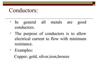
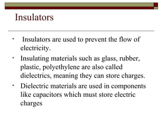
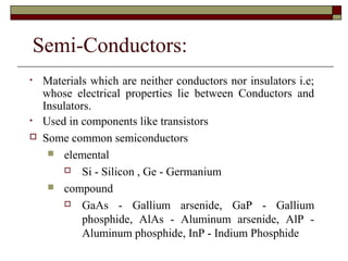
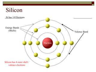
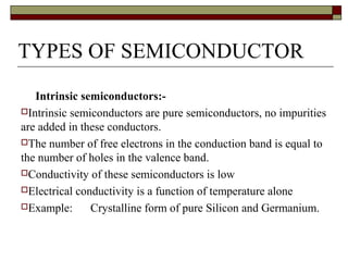
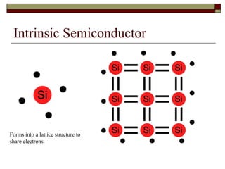
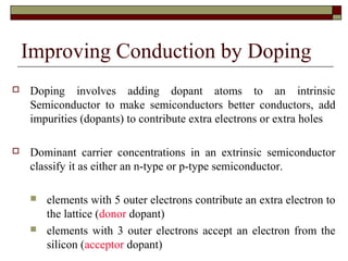
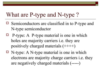


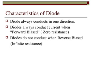
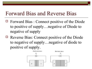


This document discusses semiconductors and their classification as conductors, insulators, or semiconductors based on their electrical properties. It describes intrinsic and extrinsic semiconductors, where intrinsic are pure and extrinsic are doped with impurities. The document focuses on silicon, explaining its crystal structure and energy bands. It also discusses doping to create n-type and p-type semiconductors, the functioning of a p-n junction diode, and forward and reverse biasing of the diode.


