Downloaded 120 times
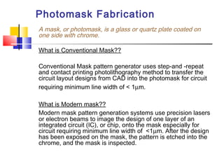
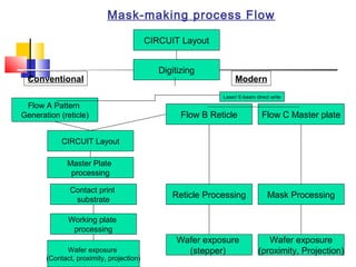
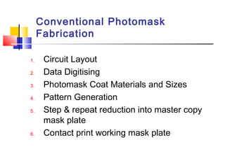
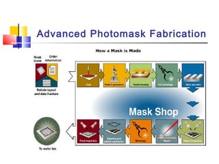

Conventional photomasks use a quartz plate coated with chrome and photolithography to transfer circuit designs onto the mask from a CAD file. Modern masks use precision lasers or electron beams to image designs requiring line widths smaller than 1 μm. The mask fabrication process involves creating a circuit layout, digitizing the data, generating patterns on a photomask or reticle, and using step-and-repeat or contact printing to produce a working mask plate for wafer exposure. X-ray masks require even finer features and use a silicon membrane with a patterned gold absorber layer.


