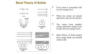
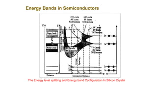
SEMICONDUCTOR PHYSICS
Electronic Materials
• The goal of electronic materials is to generate and control the flow
of an electrical current.
• Electronic materials include:
1. Conductors: have low resistance which allows electrical current flow
2. Insulators: have high resistance which suppresses electrical current flow
3. Semiconductors: can allow or suppress electrical current flow
Conductors
• Good conductors have low resistance so electrons flow through them
with ease.
• Best element conductors include:
• Copper, silver, gold, aluminum, & nickel
• Alloys are also good conductors:
• Brass & steel
• Good conductors can also be liquid:
• Salt water
Conductor Atomic Structure
• The atomic structure of good
conductors usually includes only
one electron in their outer shell.
• It is called a valence electron.
• It is easily striped from the atom,
producing current flow.
Copper Atom
Insulators
• Insulators have a high resistance so current does not flow in them.
• Good insulators include:
• Glass, ceramic, plastics, & wood
• Most insulators are compounds of several elements.
• The atoms are tightly bound to one another so electrons are difficult
to strip away for current flow.
Semiconductors
• Semiconductors are materials that essentially can be conditioned
to act as good conductors, or good insulators, or any thing in
between.
• Common elements such as carbon, silicon, and germanium are
semiconductors.
• Silicon is the best and most widely used semiconductor.
Semiconductor Valence Orbit
• The main characteristic
of a semiconductor
element is that it has
four electrons in its
outer or valence orbit.
Crystal Lattice Structure
• The unique capability of
semiconductor atoms is their
ability to link together to form a
physical structure called a crystal
lattice.
• The atoms link together with one
another sharing their outer
electrons.
• These links are called covalent
bonds.
2D Crystal Lattice Structure
3D Crystal Lattice Structure
Semiconductors can be Insulators
• If the material is pure semiconductor material like silicon, the crystal
lattice structure forms an excellent insulator since all the atoms are
bound to one another and are not free for current flow.
• Good insulating semiconductor material is referred to as intrinsic.
• Since the outer valence electrons of each atom are tightly bound
together with one another, the electrons are difficult to dislodge for
current flow.
• Silicon in this form is a great insulator.
• Semiconductor material is often used as an insulator.
Doping
• To make the semiconductor conduct electricity, other atoms
called impurities must be added.
• “Impurities” are different elements.
• This process is called doping.
Semiconductors can be Conductors
• An impurity, or element like
arsenic, has 5 valence electrons.
• Adding arsenic (doping) will allow
four of the arsenic valence
electrons to bond with the
neighboring silicon atoms.
• The one electron left over for
each arsenic atom becomes
available to conduct current flow.
Resistance Effects of Doping
• If you use lots of arsenic atoms for doping, there will be lots of extra
electrons so the resistance of the material will be low and current will
flow freely.
• If you use only a few boron atoms, there will be fewer free electrons
so the resistance will be high and less current will flow.
• By controlling the doping amount, virtually any resistance can be
achieved.
Another Way to Dope
• You can also dope a semiconductor
material with an atom such as boron
that has only 3 valence electrons.
• The 3 electrons in the outer orbit do
form covalent bonds with its
neighboring semiconductor atoms as
before. But one atom is missing from
the bond.
• This place where a fourth electron
should be is referred to as a hole.
• The hole assumes a positive charge
so it can attract electrons from some
other source.
• Holes become a type of current
carrier like the electron to support
current flow.
Types of Semiconductor Materials
• The silicon doped with extra electrons is called an “N
type” semiconductor.
• “N” is for negative, which is the charge of an electron.
• Silicon doped with material missing electrons that
produce locations called holes is called “P type”
semiconductor.
• “P” is for positive, which is the charge of a hole.
Band Theory of Solids
• Every atom is associated with
its own energy level.
• When two atoms are placed
apart then, they do not interact.
• Two atoms close together
causes particular energy level
to split into two energy levels.
• Band Theory of Solid explain
how energy bands are formed
within solid.
Energy level splitting in a solid
(a)Energy band structure of the
solid corresponding to the
actual spacing of atoms in the
body.
(b) Energy level splitting as a
function of distance.
(c) Discrete energy levels in an
isolated atom.
Energy Bands in Semiconductors
The Energy level splitting and Energy band Configuration In Silicon Crystal
Valence Band:
• “The band formed by series of energy levels containing valence electron is
called Valence Band”.
• It may be completely filled or partially filled with electrons.
Conduction Band:
• “The Band formed by energy values of free electron that have broken their
covalent bonds is called Conduction band”.
• Conduction band is the next permitted energy band.
• It may be empty or partially filled with electrons.
Forbidden energy Gap
• The energy gap between the valence band and conduction band is called the
Forbidden energy gap or Forbidden Band or Band gap.
• This band is formed by series of non permitted energy levels above the top of
valence band and below the bottom of conduction band.
• Energy gap is denoted by Eg and it is the amount of energy supplied, to excite
the electron from valence band to conduction band. It is measured in eV.

part 1_Semiconductor physics exaplanitation.pptx

  • 1.
  • 2.
    Electronic Materials • Thegoal of electronic materials is to generate and control the flow of an electrical current. • Electronic materials include: 1. Conductors: have low resistance which allows electrical current flow 2. Insulators: have high resistance which suppresses electrical current flow 3. Semiconductors: can allow or suppress electrical current flow
  • 3.
    Conductors • Good conductorshave low resistance so electrons flow through them with ease. • Best element conductors include: • Copper, silver, gold, aluminum, & nickel • Alloys are also good conductors: • Brass & steel • Good conductors can also be liquid: • Salt water
  • 4.
    Conductor Atomic Structure •The atomic structure of good conductors usually includes only one electron in their outer shell. • It is called a valence electron. • It is easily striped from the atom, producing current flow. Copper Atom
  • 5.
    Insulators • Insulators havea high resistance so current does not flow in them. • Good insulators include: • Glass, ceramic, plastics, & wood • Most insulators are compounds of several elements. • The atoms are tightly bound to one another so electrons are difficult to strip away for current flow.
  • 6.
    Semiconductors • Semiconductors arematerials that essentially can be conditioned to act as good conductors, or good insulators, or any thing in between. • Common elements such as carbon, silicon, and germanium are semiconductors. • Silicon is the best and most widely used semiconductor.
  • 7.
    Semiconductor Valence Orbit •The main characteristic of a semiconductor element is that it has four electrons in its outer or valence orbit.
  • 8.
    Crystal Lattice Structure •The unique capability of semiconductor atoms is their ability to link together to form a physical structure called a crystal lattice. • The atoms link together with one another sharing their outer electrons. • These links are called covalent bonds. 2D Crystal Lattice Structure
  • 9.
  • 10.
    Semiconductors can beInsulators • If the material is pure semiconductor material like silicon, the crystal lattice structure forms an excellent insulator since all the atoms are bound to one another and are not free for current flow. • Good insulating semiconductor material is referred to as intrinsic. • Since the outer valence electrons of each atom are tightly bound together with one another, the electrons are difficult to dislodge for current flow. • Silicon in this form is a great insulator. • Semiconductor material is often used as an insulator.
  • 11.
    Doping • To makethe semiconductor conduct electricity, other atoms called impurities must be added. • “Impurities” are different elements. • This process is called doping.
  • 12.
    Semiconductors can beConductors • An impurity, or element like arsenic, has 5 valence electrons. • Adding arsenic (doping) will allow four of the arsenic valence electrons to bond with the neighboring silicon atoms. • The one electron left over for each arsenic atom becomes available to conduct current flow.
  • 13.
    Resistance Effects ofDoping • If you use lots of arsenic atoms for doping, there will be lots of extra electrons so the resistance of the material will be low and current will flow freely. • If you use only a few boron atoms, there will be fewer free electrons so the resistance will be high and less current will flow. • By controlling the doping amount, virtually any resistance can be achieved.
  • 14.
    Another Way toDope • You can also dope a semiconductor material with an atom such as boron that has only 3 valence electrons. • The 3 electrons in the outer orbit do form covalent bonds with its neighboring semiconductor atoms as before. But one atom is missing from the bond. • This place where a fourth electron should be is referred to as a hole. • The hole assumes a positive charge so it can attract electrons from some other source. • Holes become a type of current carrier like the electron to support current flow.
  • 15.
    Types of SemiconductorMaterials • The silicon doped with extra electrons is called an “N type” semiconductor. • “N” is for negative, which is the charge of an electron. • Silicon doped with material missing electrons that produce locations called holes is called “P type” semiconductor. • “P” is for positive, which is the charge of a hole.
  • 16.
    Band Theory ofSolids • Every atom is associated with its own energy level. • When two atoms are placed apart then, they do not interact. • Two atoms close together causes particular energy level to split into two energy levels. • Band Theory of Solid explain how energy bands are formed within solid.
  • 17.
    Energy level splittingin a solid (a)Energy band structure of the solid corresponding to the actual spacing of atoms in the body. (b) Energy level splitting as a function of distance. (c) Discrete energy levels in an isolated atom.
  • 18.
    Energy Bands inSemiconductors The Energy level splitting and Energy band Configuration In Silicon Crystal
  • 19.
    Valence Band: • “Theband formed by series of energy levels containing valence electron is called Valence Band”. • It may be completely filled or partially filled with electrons. Conduction Band: • “The Band formed by energy values of free electron that have broken their covalent bonds is called Conduction band”. • Conduction band is the next permitted energy band. • It may be empty or partially filled with electrons.
  • 20.
    Forbidden energy Gap •The energy gap between the valence band and conduction band is called the Forbidden energy gap or Forbidden Band or Band gap. • This band is formed by series of non permitted energy levels above the top of valence band and below the bottom of conduction band. • Energy gap is denoted by Eg and it is the amount of energy supplied, to excite the electron from valence band to conduction band. It is measured in eV.