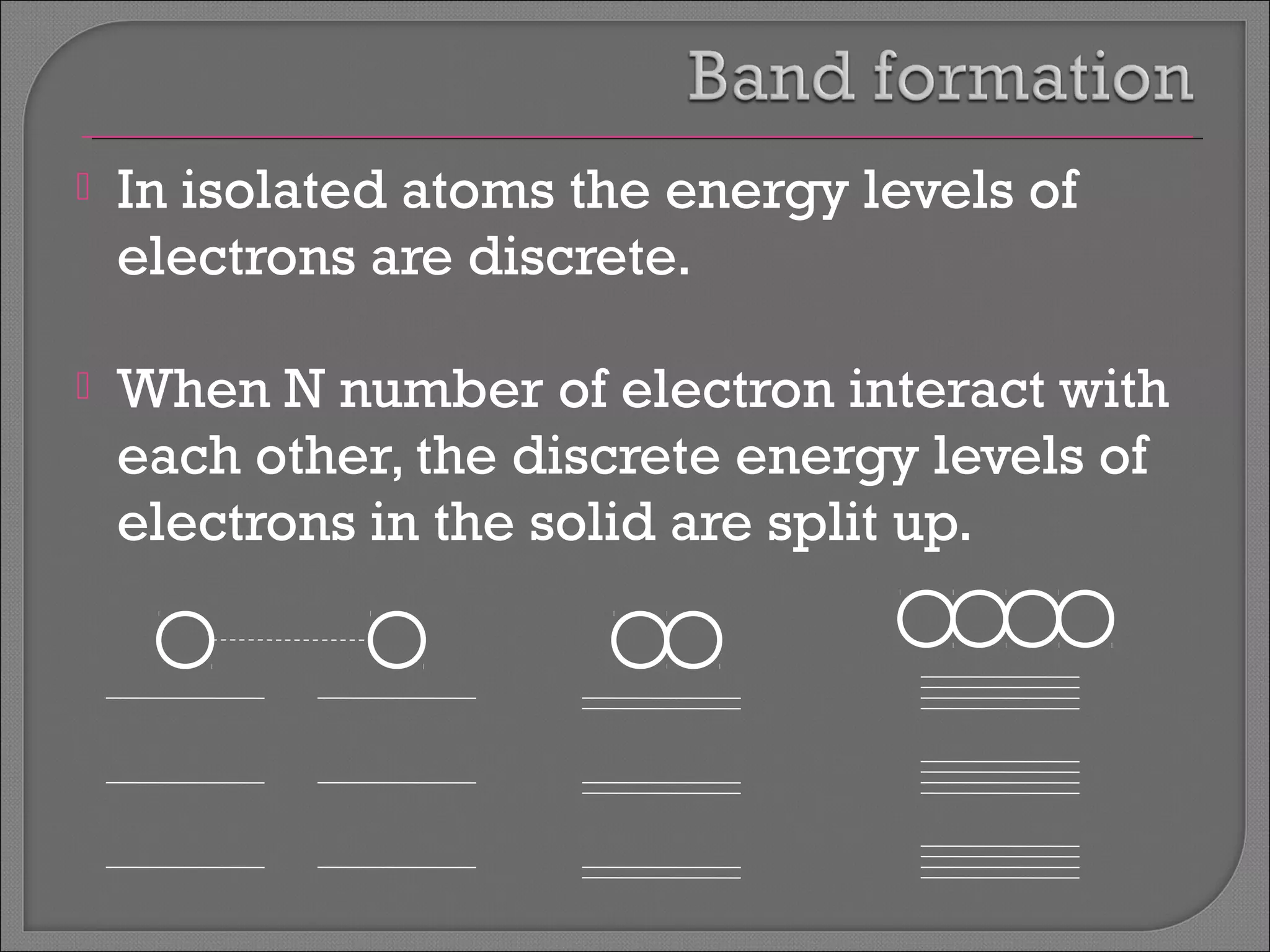
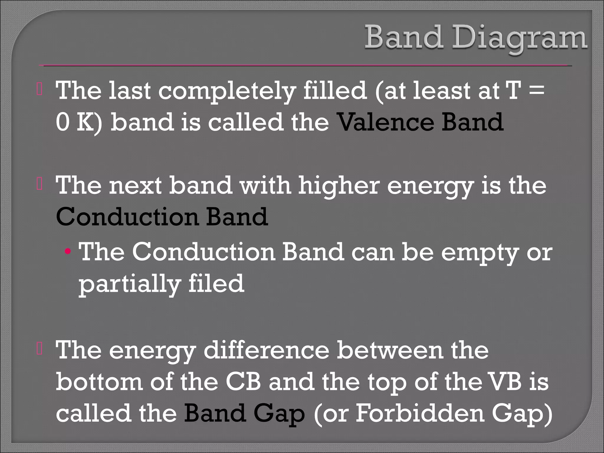
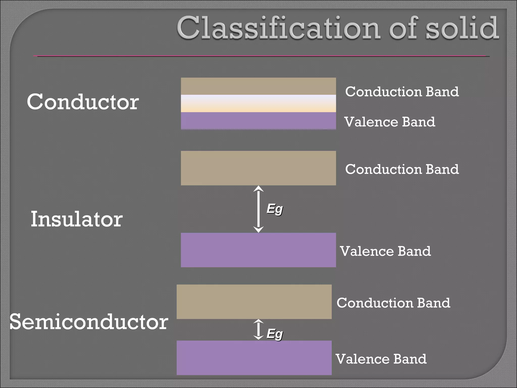
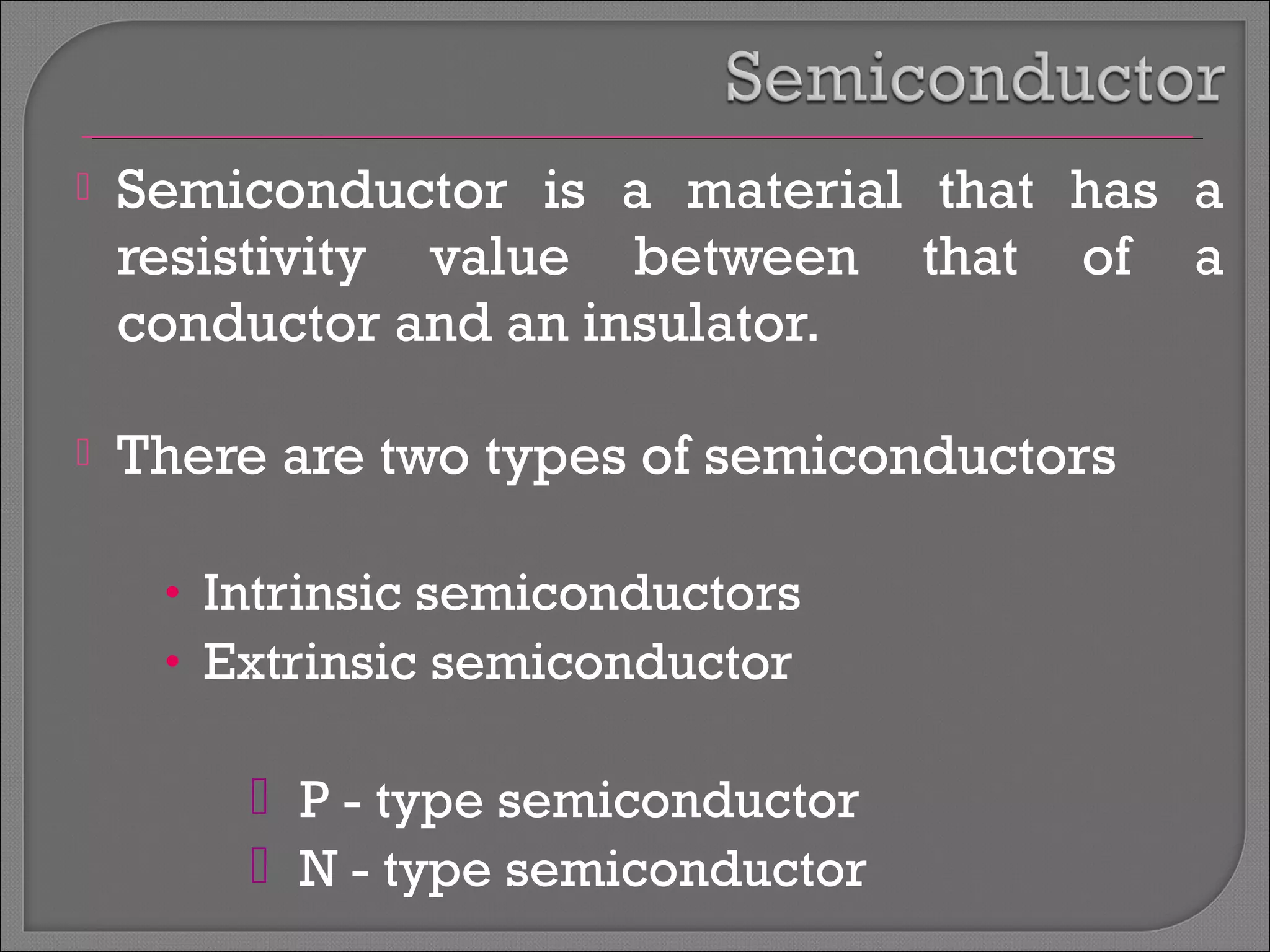
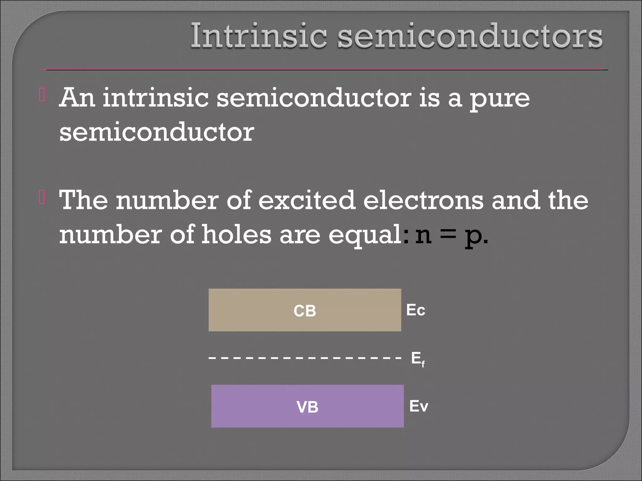
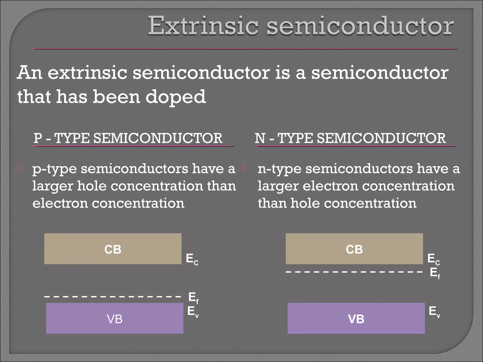
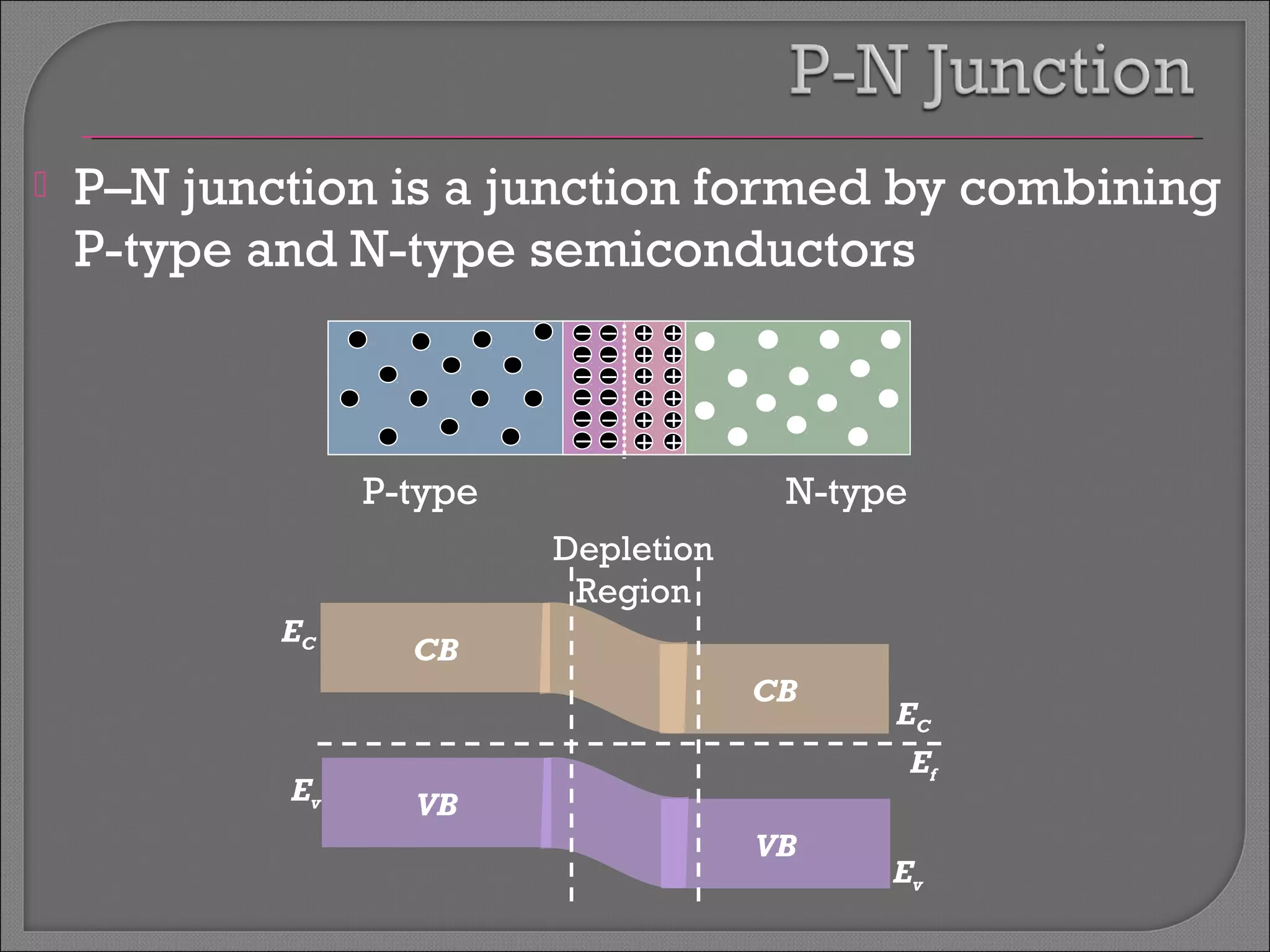
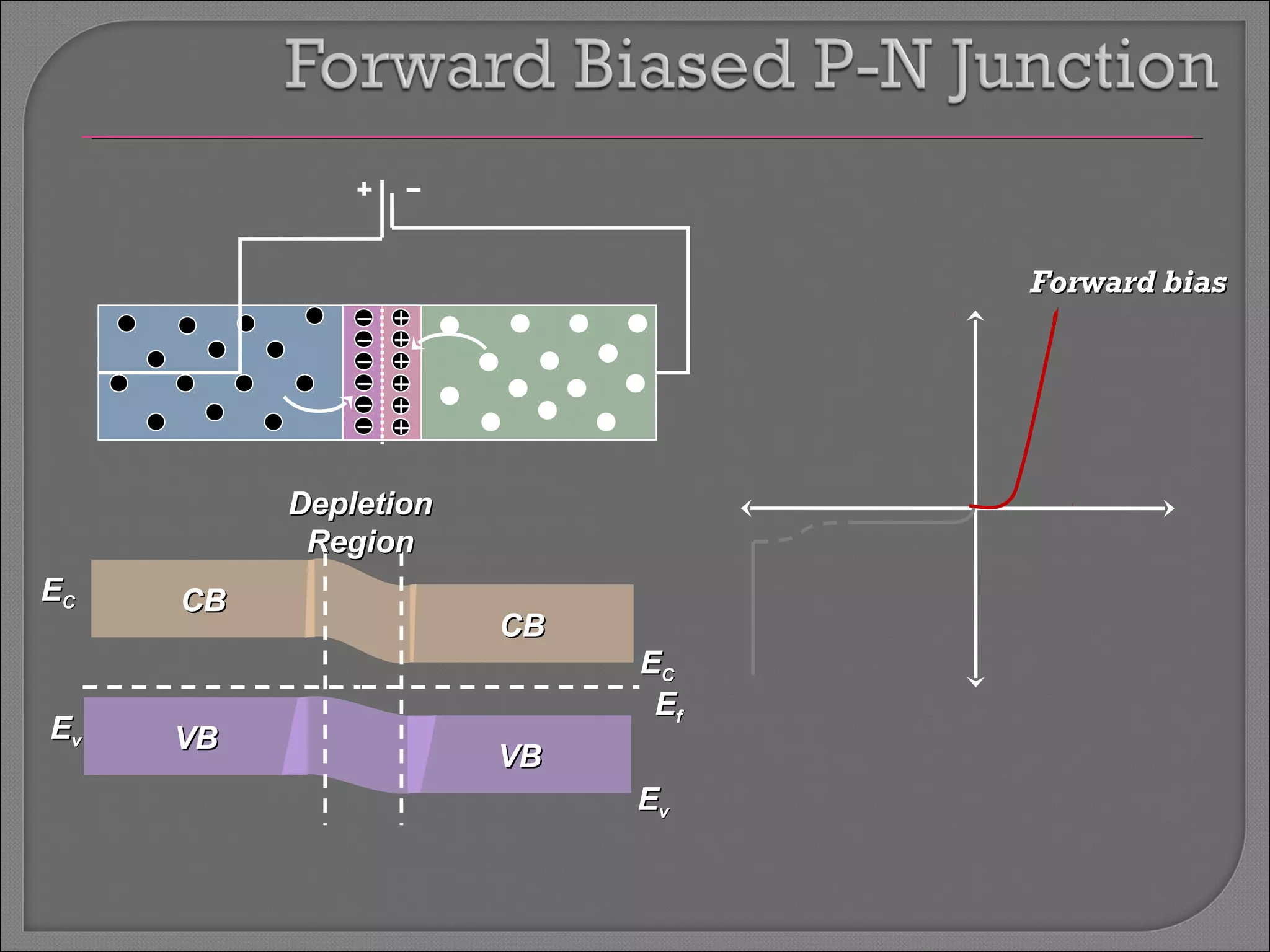
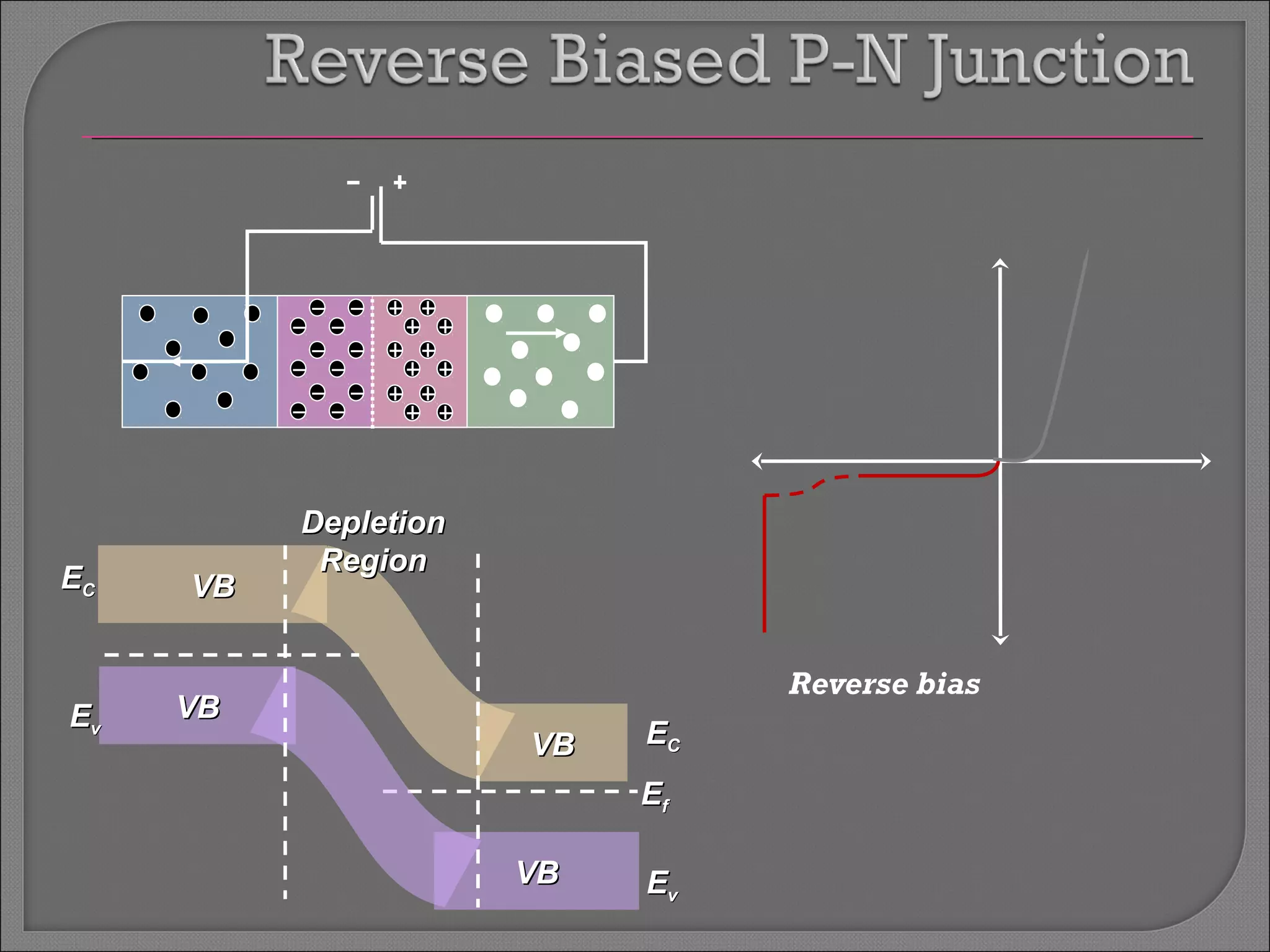
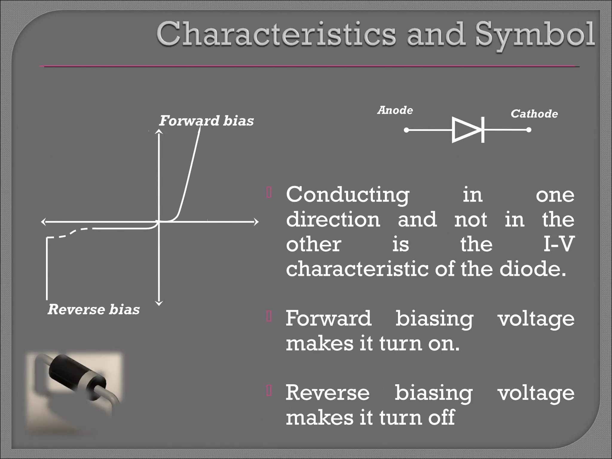
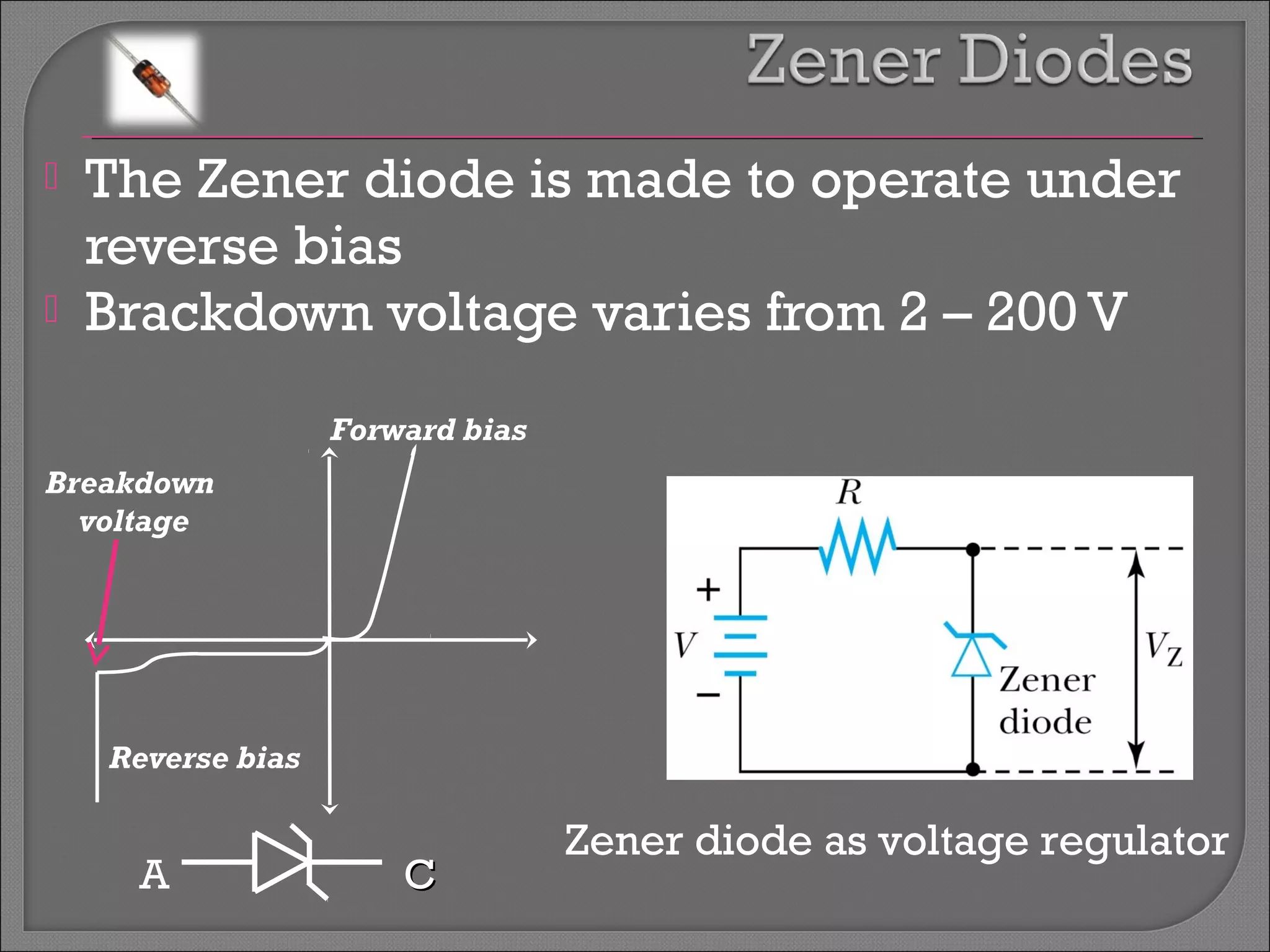
BBAANNDD TTHHEEOORRYY 
OOFF 
SSOOLLIIDD
 In isolated atoms the energy levels of 
electrons are discrete. 
 When N number of electron interact with 
each other, the discrete energy levels of 
electrons in the solid are split up.
 The last completely filled (at least at T = 
0 K) band is called the Valence Band 
 The next band with higher energy is the 
Conduction Band 
• The Conduction Band can be empty or 
partially filed 
 The energy difference between the 
bottom of the CB and the top of the VB is 
called the Band Gap (or Forbidden Gap)
Conductor 
Insulator 
Semiconductor 
Conduction Band 
Valence Band 
Conduction Band 
Valence Band 
EEgg 
Conduction Band 
Valence Band 
EEgg
 Semiconductor is a material that has a 
resistivity value between that of a 
conductor and an insulator. 
 There are two types of semiconductors 
• Intrinsic semiconductors 
• Extrinsic semiconductor 
 P - type semiconductor 
 N - type semiconductor
 An intrinsic semiconductor is a pure 
semiconductor 
 The number of excited electrons and the 
number of holes are equal: n = p. 
CB 
VB 
Ec 
Ef 
Ev
An extrinsic semiconductor is a semiconductor 
that has been doped 
P - TYPE SEMICONDUCTOR N - TYPE SEMICONDUCTOR 
 p-type semiconductors have a 
larger hole concentration than 
electron concentration 
 n-type semiconductors have a 
larger electron concentration 
than hole concentration 
CB 
EC 
Ef 
VB Ev 
CB 
EC 
Ef 
VB Ev
 P–N junction is a junction formed by combining 
P-type and N-type semiconductors 
P-type N-type 
EC 
Ev 
Ef 
Ev 
CB 
CB 
EC 
VB 
VB 
Depletion 
Region
EECC 
EEvv 
EEff 
EEvv 
CCBB 
CCBB 
EECC 
DDeepplleettiioonn 
RReeggiioonn 
VVBB VVBB 
FFoorrwwaarrdd bbiiaass
VVBB 
VVBB 
VVBB 
EECC 
EEvv 
EECC 
EEff 
EEvv 
VVBB 
DDeepplleettiioonn 
RReeggiioonn 
Reverse bias
Anode Cathode 
 Conducting in one 
direction and not in the 
other is the I-V 
characteristic of the diode. 
 Forward biasing voltage 
makes it turn on. 
 Reverse biasing voltage 
makes it turn off 
Forward bias 
Reverse bias
 The Zener diode is made to operate under 
reverse bias 
 Brackdown voltage varies from 2 – 200 V 
Forward bias 
Reverse bias 
Zener diode as voltage regulator 
Breakdown 
voltage 
A CC
 Variable reactance diode 
 Voltage-controlled capacitance of a p n 
junction can be used in tuning stage of a 
radio or TV receiver. 
Anode Cathode 
Symbol 
CT 
VR 
CT ∞ 1/√VR 
w ∞ √VR
 Many of these diodes involve direct 
bandgap semiconductors. 
 Devices to convert optical energy to 
electrical energy 
• photodetectors: generate electrical signal 
• Solar cells: generate electrical power 
 Devices to convert electrical energy to 
optical energy 
• light emitting diodes (LEDs) 
• laser diodes
 movement of carriers across their depletion 
region emits photons of light energy 
 For visible light output, the bandgap should 
be between 1.8 and 3.1 eV. 
P type 
N type 
Ohmic Contact 
AA CC 
Symbol
 Photodiodes are sensitive to light. 
 In Photoconductive mode the saturation 
current increases in proportion to the 
intensity of the received light. 
• An important characteristic of any 
photo-detector. Measures how the 
photocurrent, IL varies with the 
wavelength of incident light. 
AA CC 
Symbol 
V 
I 
Increasing 
light intensity
 In Photovoltaic mode, when the pn junction 
is exposed to a certain wavelength of light, 
the diode generates voltage and can be 
used as an energy source. 
 This type of diode is used in the production 
of solar power. 
 Also known as 
Solar cells
 Solar cells are large area pn-junction 
diodes designed specifically to avoid 
energy losses. 
• Voc= the open circuit voltage 
• Isc = current when device is 
short circuited 
h = power conversion 
efficiency 
= (Im Vm)/Pin 
I 
Voc 
VA 
Vm 
– Isc 
–Im
Thanks……….

Band theory of solid

  • 1.
  • 2.
     In isolatedatoms the energy levels of electrons are discrete.  When N number of electron interact with each other, the discrete energy levels of electrons in the solid are split up.
  • 3.
     The lastcompletely filled (at least at T = 0 K) band is called the Valence Band  The next band with higher energy is the Conduction Band • The Conduction Band can be empty or partially filed  The energy difference between the bottom of the CB and the top of the VB is called the Band Gap (or Forbidden Gap)
  • 4.
    Conductor Insulator Semiconductor Conduction Band Valence Band Conduction Band Valence Band EEgg Conduction Band Valence Band EEgg
  • 5.
     Semiconductor isa material that has a resistivity value between that of a conductor and an insulator.  There are two types of semiconductors • Intrinsic semiconductors • Extrinsic semiconductor  P - type semiconductor  N - type semiconductor
  • 6.
     An intrinsicsemiconductor is a pure semiconductor  The number of excited electrons and the number of holes are equal: n = p. CB VB Ec Ef Ev
  • 7.
    An extrinsic semiconductoris a semiconductor that has been doped P - TYPE SEMICONDUCTOR N - TYPE SEMICONDUCTOR  p-type semiconductors have a larger hole concentration than electron concentration  n-type semiconductors have a larger electron concentration than hole concentration CB EC Ef VB Ev CB EC Ef VB Ev
  • 8.
     P–N junctionis a junction formed by combining P-type and N-type semiconductors P-type N-type EC Ev Ef Ev CB CB EC VB VB Depletion Region
  • 9.
    EECC EEvv EEff EEvv CCBB CCBB EECC DDeepplleettiioonn RReeggiioonn VVBB VVBB FFoorrwwaarrdd bbiiaass
  • 10.
    VVBB VVBB VVBB EECC EEvv EECC EEff EEvv VVBB DDeepplleettiioonn RReeggiioonn Reverse bias
  • 11.
    Anode Cathode Conducting in one direction and not in the other is the I-V characteristic of the diode.  Forward biasing voltage makes it turn on.  Reverse biasing voltage makes it turn off Forward bias Reverse bias
  • 12.
     The Zenerdiode is made to operate under reverse bias  Brackdown voltage varies from 2 – 200 V Forward bias Reverse bias Zener diode as voltage regulator Breakdown voltage A CC
  • 13.
     Variable reactancediode  Voltage-controlled capacitance of a p n junction can be used in tuning stage of a radio or TV receiver. Anode Cathode Symbol CT VR CT ∞ 1/√VR w ∞ √VR
  • 14.
     Many ofthese diodes involve direct bandgap semiconductors.  Devices to convert optical energy to electrical energy • photodetectors: generate electrical signal • Solar cells: generate electrical power  Devices to convert electrical energy to optical energy • light emitting diodes (LEDs) • laser diodes
  • 15.
     movement ofcarriers across their depletion region emits photons of light energy  For visible light output, the bandgap should be between 1.8 and 3.1 eV. P type N type Ohmic Contact AA CC Symbol
  • 16.
     Photodiodes aresensitive to light.  In Photoconductive mode the saturation current increases in proportion to the intensity of the received light. • An important characteristic of any photo-detector. Measures how the photocurrent, IL varies with the wavelength of incident light. AA CC Symbol V I Increasing light intensity
  • 17.
     In Photovoltaicmode, when the pn junction is exposed to a certain wavelength of light, the diode generates voltage and can be used as an energy source.  This type of diode is used in the production of solar power.  Also known as Solar cells
  • 18.
     Solar cellsare large area pn-junction diodes designed specifically to avoid energy losses. • Voc= the open circuit voltage • Isc = current when device is short circuited h = power conversion efficiency = (Im Vm)/Pin I Voc VA Vm – Isc –Im
  • 19.