Download as PPSX, PPTX
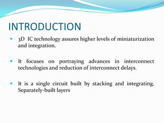
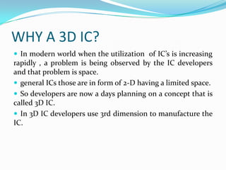
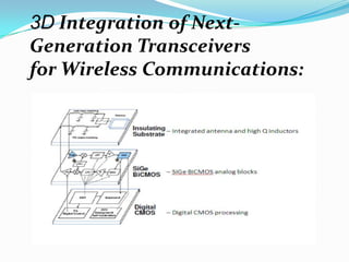


This document discusses 3D integrated circuits (3D ICs). It begins by introducing 3D ICs and how they allow for higher levels of miniaturization and integration by stacking separately built circuit layers. It then discusses why 3D ICs are needed due to limited space in traditional 2D chip designs. Key benefits of 3D ICs include reduced wire lengths, increased number of nearest neighbors for transistors, and heterogeneous integration. However, 3D ICs also present challenges related to thermal issues, reliability, and design complexity that must be addressed. The document surveys applications and advances in 3D ICs.