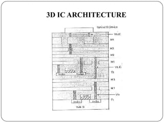
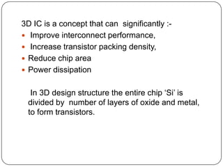
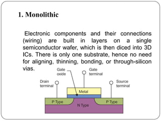
A
                                    Presentation
                                         On
                                      “3D ICs”
        Presented in partial fulfillment of Bachelor’s Degree in Technology
                         Rajasthan Technical University
                                        Kota


                                  Session: 2011-2012

PRESENTED TO:                                                      PRESENTED
BY:
Garima Mathur                                                 Dinesh Kumar
 HOD, Deptt. of ECE                                    (EC08033)

           Department of Electronics and Communication Engineering
                        Jaipur Engineering College, Kukas
CONTENTS
• INTRODUCTION
• IDEA FOR 3D IC
• LIMITED PERFORMANCE OF 3D IC
• 3D ARCHITECTURE
• MANUFACTURING TECHNOLOGY OF 3D ICs
• ADVANTAGES OF 3D ARCHITECTURE
• PERFORMANCE CHARACTERISTICS
• CONCERNS IN 3D CIRCUITS
• PRESENT SCENARIO IN 3D IC INDUSTRY
• CONCLUSION
INTRODUCTION


In electronics, a three-dimensional integrated circuit is a chip
in which two or more layers of active electronic components are
integrated both vertically and horizontally into a single circuit.

In contrast, a 3D IC is a single chip in which all components on
the layers communicate using on-chip signaling, whether
vertically or horizontally.
IDEA FOR 3D IC

  The large growth of computer and information
 technology industry is depending on VLSI circuits
 with increasing functionality and performance at
 minimum cost and power dissipation and 2D ICs
 generate various gate delays and interconnection
 delay.

  So to reduce these delays and total power
 consumption,
  3D IC technology is introduced.

 Intel introduced 80 core chip in 2007 which run on
 the frequency of 1.4GHz.
LIMITED PERFORMANCE OF 2D ICs


 As we try to increase the performance and
efficiency of chip, the complexity of chip design
increases and this requires more and more
transistors. So the final size of the circuit and
delays increases.
 The losses increases with large interconnection
because the capacitance and resistances are
generated in between the clad and copper.
3D IC ARCHITECTURE
3D IC is a concept that can significantly :-
 Improve interconnect performance,
 Increase transistor packing density,
 Reduce chip area
 Power dissipation


  In 3D design structure the entire chip ‘Si’ is
 divided by number of layers of oxide and metal,
 to form transistors.
MANUFACTURING TECHNOLOGY OF 3D ICs


 There are four ways to built 3D ICs :-
 1. Monolithic
 2. Wafer on wafer
 3. Die on wafer
 4. Die on die
1. Monolithic

  Electronic components and their connections
 (wiring) are built in layers on a single
 semiconductor wafer, which is then diced into 3D
 ICs. There is only one substrate, hence no need
 for aligning, thinning, bonding, or through-silicon
 vias.
2. Wafer on wafer
  Electronic components are built on two or more
 semiconductor wafers, which are then aligned,
 bonded, and diced into 3D ICs.
3. Die on wafer
Electronic components are built on two
semiconductor wafers. One wafer is diced aligned
and bonded onto die sites of the second wafer.
4.Die on die
Electronic components are built on multiple dice,
which are then aligned and bonded.
One advantage of die-on-die is that each
component die can be tested first, so that one
bad die does not ruin an entire stack
AVANTAGES OF 3D ARCHITECTURE

 3D integration can reduce the wiring, thereby
  reducing the capacitances, power dissipation and
  chip area improves performance.
 Digital and analog circuits can be formed with
  better noise performance.
 It more cost effective then 2D integration.
PERFORMANCE CHARACTERISTICS

1. TIMING
2. ENERGY


      With shorter interconnects in 3D ICs, both
     switching energy and cycle time are
     expected to be reduced
1. TIMING


 The graph shows the
 results of a reduction in
 wire length due to 3D
 routing.


 Reduction in the
 interconnect lengths
 reduces RC delays and
 increase chip timing
 performance
2. ENERGY PERFOMANCE

 The graph shows
 the reduction in a
 normalized energy
 consumption with
 number of wire
 layers.
CONCERNS IN 3D CIRCUIT
 Thermal Issues in 3D-circuits
 Reliability Issues
PRESENT SCENARIO IN 3D IC INDUSTRY

Many companies like MIT (USA), IBM are doing
 research on 3D IC technology and they are going
 to introduce cheaper chips for certain
 applications, like memory used in digital cameras,
 cell phones, handheld gaming devices etc.

The original cost will be 10 times lesser than the
 current ones.
CONCLUSION
 3D ICs will be the first of a new generation of
dense, inexpensive chips having less delay and
interconnection losses that will replace the
conventional storage and recording media.
QUERIES???

3D ICs

  • 1.
    A Presentation On “3D ICs” Presented in partial fulfillment of Bachelor’s Degree in Technology Rajasthan Technical University Kota Session: 2011-2012 PRESENTED TO: PRESENTED BY: Garima Mathur Dinesh Kumar HOD, Deptt. of ECE (EC08033) Department of Electronics and Communication Engineering Jaipur Engineering College, Kukas
  • 2.
    CONTENTS • INTRODUCTION • IDEAFOR 3D IC • LIMITED PERFORMANCE OF 3D IC • 3D ARCHITECTURE • MANUFACTURING TECHNOLOGY OF 3D ICs • ADVANTAGES OF 3D ARCHITECTURE • PERFORMANCE CHARACTERISTICS • CONCERNS IN 3D CIRCUITS • PRESENT SCENARIO IN 3D IC INDUSTRY • CONCLUSION
  • 3.
    INTRODUCTION In electronics, athree-dimensional integrated circuit is a chip in which two or more layers of active electronic components are integrated both vertically and horizontally into a single circuit. In contrast, a 3D IC is a single chip in which all components on the layers communicate using on-chip signaling, whether vertically or horizontally.
  • 4.
    IDEA FOR 3DIC The large growth of computer and information technology industry is depending on VLSI circuits with increasing functionality and performance at minimum cost and power dissipation and 2D ICs generate various gate delays and interconnection delay. So to reduce these delays and total power consumption, 3D IC technology is introduced.  Intel introduced 80 core chip in 2007 which run on the frequency of 1.4GHz.
  • 5.
    LIMITED PERFORMANCE OF2D ICs As we try to increase the performance and efficiency of chip, the complexity of chip design increases and this requires more and more transistors. So the final size of the circuit and delays increases. The losses increases with large interconnection because the capacitance and resistances are generated in between the clad and copper.
  • 6.
  • 7.
    3D IC isa concept that can significantly :-  Improve interconnect performance,  Increase transistor packing density,  Reduce chip area  Power dissipation In 3D design structure the entire chip ‘Si’ is divided by number of layers of oxide and metal, to form transistors.
  • 8.
    MANUFACTURING TECHNOLOGY OF3D ICs There are four ways to built 3D ICs :- 1. Monolithic 2. Wafer on wafer 3. Die on wafer 4. Die on die
  • 9.
    1. Monolithic Electronic components and their connections (wiring) are built in layers on a single semiconductor wafer, which is then diced into 3D ICs. There is only one substrate, hence no need for aligning, thinning, bonding, or through-silicon vias.
  • 10.
    2. Wafer onwafer Electronic components are built on two or more semiconductor wafers, which are then aligned, bonded, and diced into 3D ICs.
  • 11.
    3. Die onwafer Electronic components are built on two semiconductor wafers. One wafer is diced aligned and bonded onto die sites of the second wafer.
  • 12.
    4.Die on die Electroniccomponents are built on multiple dice, which are then aligned and bonded. One advantage of die-on-die is that each component die can be tested first, so that one bad die does not ruin an entire stack
  • 13.
    AVANTAGES OF 3DARCHITECTURE  3D integration can reduce the wiring, thereby reducing the capacitances, power dissipation and chip area improves performance.  Digital and analog circuits can be formed with better noise performance.  It more cost effective then 2D integration.
  • 14.
    PERFORMANCE CHARACTERISTICS 1. TIMING 2.ENERGY With shorter interconnects in 3D ICs, both switching energy and cycle time are expected to be reduced
  • 15.
    1. TIMING  Thegraph shows the results of a reduction in wire length due to 3D routing.  Reduction in the interconnect lengths reduces RC delays and increase chip timing performance
  • 16.
    2. ENERGY PERFOMANCE The graph shows the reduction in a normalized energy consumption with number of wire layers.
  • 17.
    CONCERNS IN 3DCIRCUIT  Thermal Issues in 3D-circuits  Reliability Issues
  • 18.
    PRESENT SCENARIO IN3D IC INDUSTRY Many companies like MIT (USA), IBM are doing research on 3D IC technology and they are going to introduce cheaper chips for certain applications, like memory used in digital cameras, cell phones, handheld gaming devices etc. The original cost will be 10 times lesser than the current ones.
  • 19.
    CONCLUSION 3D ICswill be the first of a new generation of dense, inexpensive chips having less delay and interconnection losses that will replace the conventional storage and recording media.
  • 21.