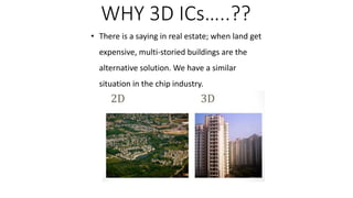
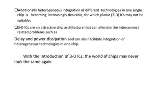
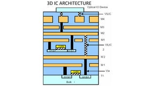
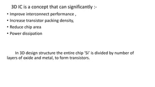
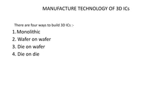
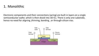
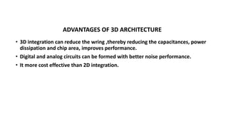
3D INTEGRATED CIRCUITS
BY
MUFEED UL ISLAM
ECE-13-64
• There is a saying in real estate; when land get
expensive, multi-storied buildings are the
alternative solution. We have a similar
situation in the chip industry.
WHY 3D ICs…..??
Additionally heterogeneous integration of different technologies in one single
chip is becoming increasingly desirable, for which planar (2-D) ICs may not be
suitable.
3-D ICs are an attractive chip architecture that can alleviate the interconnect
related problems such as
Delay and power dissipation and can also facilitate integration of
heterogeneous technologies in one chip.
With the Introduction of 3-D ICs, the world of chips may never
look the same again.
Contents
INTRODUCTION
IDEA FOR 3D IC
LIMITED PERFORMANCE OF 3D IC
3D ARCHITECTURE
MANUFACTURING TECHNOLOGY OF 3D Ics
ADVANTAGES OF 3D ARCHITECTURE
PERFORMANCE CHARACTERISTICS
CONCERN IN 3D CIRCUITS
PRESENT SENARIO IN 3D INDUSTRY
CONCLUSION
Introduction
• In electronics, a three-dimensional integrated circuit is a chip in which
two or more layers of active electronic components are integrated
both vertically and horizontally into a single circuit.
• In contrast , a 3D IC is a single chip in which all components on the
layers communicate using on-chip signaling, whether vertically or
horizontally.
IDEA FOR 3D IC
The large growth of computer and information technology industry is
depending on VLSI circuits with increasing functionality and
performance at the minimum cost and power dissipation and 2D ICs
generate various gate delays and interconnection delay.
So to reduce these delays and total power consumption ,
3D IC technology is introduced.
• Intel introduced 80 core chip in 2007 which run on the frequency of
1.4GHz.
LIMITED PERFORMANCE OF 2D ICs
• As we try to increase the performance and efficiency of chip, the
complexity of chip design increases and this requires more and
more transistors . So the final size of the circuit and delay increases.
• The losses increases with large interconnection because the
capacitance and resistances are generated in between the clad and
the copper.
3D IC ARCHITECTURE
3D IC is a concept that can significantly :-
• Improve interconnect performance ,
• Increase transistor packing density,
• Reduce chip area
• Power dissipation
In 3D design structure the entire chip ‘Si’ is divided by number of
layers of oxide and metal, to form transistors.
MANUFACTURE TECHNOLOGY OF 3D ICs
There are four ways to build 3D ICs :-
1.Monolithic
2. Wafer on wafer
3. Die on wafer
4. Die on die
1. Monolithic
Electronic components and their connections (wring) are built in layers on a single
semiconductor wafer, which is then diced into 3D ICs. There is only one substrate,
hence no need for aligning ,thinning, bonding , or through-silicon vias.
2. Wafer on wafer
Electronic components are built on two or more semiconductor wafers , which are
then aligned, bonded, and diced into 3D ICs.
Each wafer may be thinned before or after bonding.
3. Die on wafer
Electronic components are built on two semiconductor wafers. One wafer is diced
aligned and bonded onto die sites of the second wafer.
4. Die on die
Electronic components are built on multiple dice, which are then
aligned and bonded.
One advantage of die-on-die is that each component die can be tested
first, so that one bad dies does not ruin on entire stack
ADVANTAGES OF 3D ARCHITECTURE
• 3D integration can reduce the wring ,thereby reducing the capacitances, power
dissipation and chip area, improves performance.
• Digital and analog circuits can be formed with better noise performance.
• It more cost effective than 2D integration.
PERFORMANCE CHARACTERISTICS
1. TIMING
2. ENERGY
With shorter interconnects in 3D ICs, both switching energy and cycle
time are expected to be reduced.
1. TIMING
• The graph shows the results of a reduction in wire length due to 3D routing.
• Reduction in the interconnect lengths reduces RC
delays and increase chip timing performance
2. ENERGY PERFORMANCE
• Energy dissipation decreases with the number of layers used in the design
• The graph shows the reduction in a normalized energy consumption with number of wire layers.
CONCERNS IN 3D CIRCUIT
• Thermal issues in 3D-circuits
• Reliability issues
PRESENT SCENARIO IN 3D IC INDUSTRY
Many companies like MIT (USA), IBM are doing research on 3D IC technology and
they are doing
Research on 3D IC technology and they are going to introduce cheaper chips for
certain applications, like memory used in digital cameras, cell phones, handled
gaming devices etc.
The original cost will be 10 times lesser than the current ones.
CONCLUSION
3D ICs will be the first of new generation of dense, inexpensive chips
having less delay and interconnection losses that will replace the
conventional storage and recording media.
THANK
YOU…mufeedulislam@gmail.com

3D INTEGRATED CIRCUITS

  • 1.
  • 2.
    • There isa saying in real estate; when land get expensive, multi-storied buildings are the alternative solution. We have a similar situation in the chip industry. WHY 3D ICs…..??
  • 3.
    Additionally heterogeneous integrationof different technologies in one single chip is becoming increasingly desirable, for which planar (2-D) ICs may not be suitable. 3-D ICs are an attractive chip architecture that can alleviate the interconnect related problems such as Delay and power dissipation and can also facilitate integration of heterogeneous technologies in one chip. With the Introduction of 3-D ICs, the world of chips may never look the same again.
  • 4.
    Contents INTRODUCTION IDEA FOR 3DIC LIMITED PERFORMANCE OF 3D IC 3D ARCHITECTURE MANUFACTURING TECHNOLOGY OF 3D Ics ADVANTAGES OF 3D ARCHITECTURE PERFORMANCE CHARACTERISTICS CONCERN IN 3D CIRCUITS PRESENT SENARIO IN 3D INDUSTRY CONCLUSION
  • 5.
    Introduction • In electronics,a three-dimensional integrated circuit is a chip in which two or more layers of active electronic components are integrated both vertically and horizontally into a single circuit. • In contrast , a 3D IC is a single chip in which all components on the layers communicate using on-chip signaling, whether vertically or horizontally.
  • 6.
    IDEA FOR 3DIC The large growth of computer and information technology industry is depending on VLSI circuits with increasing functionality and performance at the minimum cost and power dissipation and 2D ICs generate various gate delays and interconnection delay. So to reduce these delays and total power consumption , 3D IC technology is introduced. • Intel introduced 80 core chip in 2007 which run on the frequency of 1.4GHz.
  • 7.
    LIMITED PERFORMANCE OF2D ICs • As we try to increase the performance and efficiency of chip, the complexity of chip design increases and this requires more and more transistors . So the final size of the circuit and delay increases. • The losses increases with large interconnection because the capacitance and resistances are generated in between the clad and the copper.
  • 8.
  • 9.
    3D IC isa concept that can significantly :- • Improve interconnect performance , • Increase transistor packing density, • Reduce chip area • Power dissipation In 3D design structure the entire chip ‘Si’ is divided by number of layers of oxide and metal, to form transistors.
  • 10.
    MANUFACTURE TECHNOLOGY OF3D ICs There are four ways to build 3D ICs :- 1.Monolithic 2. Wafer on wafer 3. Die on wafer 4. Die on die
  • 11.
    1. Monolithic Electronic componentsand their connections (wring) are built in layers on a single semiconductor wafer, which is then diced into 3D ICs. There is only one substrate, hence no need for aligning ,thinning, bonding , or through-silicon vias.
  • 12.
    2. Wafer onwafer Electronic components are built on two or more semiconductor wafers , which are then aligned, bonded, and diced into 3D ICs. Each wafer may be thinned before or after bonding.
  • 13.
    3. Die onwafer Electronic components are built on two semiconductor wafers. One wafer is diced aligned and bonded onto die sites of the second wafer.
  • 14.
    4. Die ondie Electronic components are built on multiple dice, which are then aligned and bonded. One advantage of die-on-die is that each component die can be tested first, so that one bad dies does not ruin on entire stack
  • 15.
    ADVANTAGES OF 3DARCHITECTURE • 3D integration can reduce the wring ,thereby reducing the capacitances, power dissipation and chip area, improves performance. • Digital and analog circuits can be formed with better noise performance. • It more cost effective than 2D integration.
  • 16.
    PERFORMANCE CHARACTERISTICS 1. TIMING 2.ENERGY With shorter interconnects in 3D ICs, both switching energy and cycle time are expected to be reduced.
  • 17.
    1. TIMING • Thegraph shows the results of a reduction in wire length due to 3D routing. • Reduction in the interconnect lengths reduces RC delays and increase chip timing performance
  • 18.
    2. ENERGY PERFORMANCE •Energy dissipation decreases with the number of layers used in the design • The graph shows the reduction in a normalized energy consumption with number of wire layers.
  • 19.
    CONCERNS IN 3DCIRCUIT • Thermal issues in 3D-circuits • Reliability issues
  • 20.
    PRESENT SCENARIO IN3D IC INDUSTRY Many companies like MIT (USA), IBM are doing research on 3D IC technology and they are doing Research on 3D IC technology and they are going to introduce cheaper chips for certain applications, like memory used in digital cameras, cell phones, handled gaming devices etc. The original cost will be 10 times lesser than the current ones.
  • 21.
    CONCLUSION 3D ICs willbe the first of new generation of dense, inexpensive chips having less delay and interconnection losses that will replace the conventional storage and recording media.
  • 22.