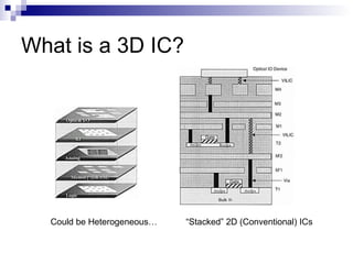
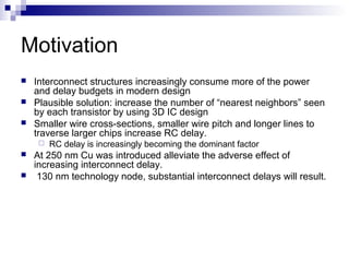
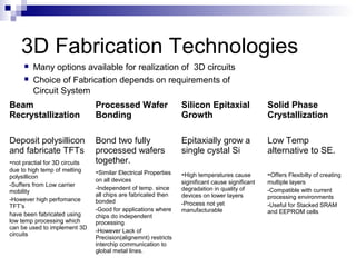
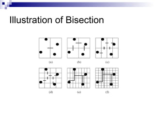
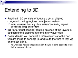
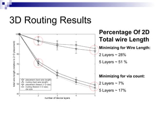
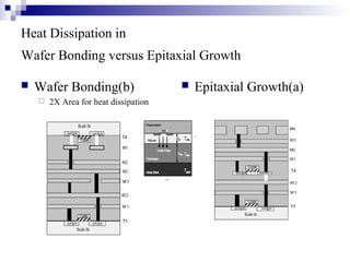
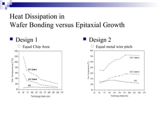
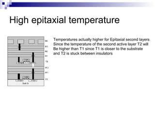
3D IC technology stacks multiple silicon layers vertically using through-silicon vias to connect the layers. This reduces interconnect length and delay. Motivations for 3D ICs include alleviating increasing interconnect delay issues and increasing the number of "nearest neighbors" for each transistor. Fabrication approaches include wafer bonding and epitaxial growth. Performance benefits include reduced timing delay and energy due to shorter interconnects. Design tools are needed to enable 3D IC design.
3D IC Presented by Tripti Kumari, School of Engineering, CUSATthevijayps
A 3D Integrated Circuit is a chip that has active electronic components stacked on one or more layers that are integrated both vertically and horizontally forming a single circuit.
In the 3-D design architecture, an entire chip is divided into a number of blocks, and each block is placed on a separate layer of Si that are stacked on top of each other.
In a generic 3D IC structure, each die is stacked on top of another and communicated by Through-Silicon Vias (TSVs).
Architectural issues
Traditional shared buses do not scale well – bandwidth saturation
Chip IO is pad limited
Physical issues
On-chip Interconnects become increasingly slower w.r.t. logic
IOs are increasingly expensive
Consequences
Performance losses
Power/Energy cost
Design closure issues or infeasibility
Reduced wire length
Total wire length
Larger circuits produce more improvement
Lower power per transistor
Decreased interconnect delay
Higher transistor packing densities
Smaller chip areas
There are four ways to build a 3D IC:
Monolithic
Wafer-on-Wafer
Die-on-Wafer
Die On Die
At runtime, thermal variations will introduce additional time-varying clock skew, further increasing design uncertainty
2 - Thermal Issues In 3-D ICs
Due to reduction in chip size of a 3D implementation, 3D circuits exhibit a sharp increase in power density
Analysis of Thermal problems in 3D is necessary to evaluate thermal robustness of different 3D technology and design options.
3 - Reliability Issues In 3-D ICs
Electro thermal and Thermo-mechanical effects between various active layers can influence electro-migration and chip performance
Die yield issues may arise due to mismatches between die yields of different layers, which affect net yield of 3D chips.
TSV check on reset
Control use dedicated Vias in order to establish which vias are corrupted.
If 1, 2 and 3 TSVs are OK, the control set the enable signal set_to and set_from: broken path are skipped!
Pads routing shift as show in the figure
Need to define The handling protocol during the TSVs check
3D IC design is a relief to interconnect driven IC design.
Still many manufacturing and technological difficulties
Physical Design needs to consider the multiple layers of Silicon available.
Optimization of both temperature and wirelength
Placement and routing algorithms need to be modified
[1] J. Davis, et al., "Interconnect limits on gigascale integration (GSI) in the 21st century," Proceedings of the IEEE , vol.89, no.3, pp.305-324, Mar 2001.
[2] Banerjee, K.; Souri, S.J.; Kapur, P.; Saraswat, K.C.; , "3-D ICs: a novel chip design for improving deep- submicrometer interconnect performance and systems-on-chip integration," Proceedings of the IEEE , vol.89, no.5, pp.602-633, May 2001.
3-D ICs are an attractive chip architecture that can alleviate the interconnect related problems such as delay and power dissipation and can also facilitate integration of heterogeneous technologies in one chip (SoC).
3D Integrated Circuits and their economic feasibilityJeffrey Funk
These slides use concepts from my (Jeff Funk) course entitled analyzing hi-tech opportunities to analyze how the economic feasibility of 3D integrated circuits (ICs) is becoming better and this will enable the continuation of Moore’s Law. 3D ICs involve the stacking of transistors and memory cells on top of each other in order to increase the number of transistors per chip area and thus continue Moore’s Law. As opposed to attempting to further reduce the feature sizes, engineers build up. They increase the number of layers of transistors and memory cells just as they have increased the number of layers of metal interconnect. To do this, they connect the different layers of transistors and memory cells with so-called Vias that are fabricated from copper.
IC suppliers began shipping 3D ICs in 2006 and these shipments have gradually grown and expanded from simple structured ICs such as image sensors to power ICs, and more recently memories, microprocessors, and ASICs. It is easier to increase the number of layers on simple than complex structured ICs. The global 3D IC market is expected to grow from $2.21 billion in 2009 to $6.55 billion in 2016 at a compound annual rate of 16.9% from 2011 to 2016.
Although it is hard to compare actual 2D and 3D ICs, simulations allow us to easily do such comparisons. For example, simulations found that chip area is almost 50% less and the metal length is about 28% less for 3D than 2D chips. The shorter metal length means that speeds will be faster since the electrons have less distance to travel. Simulations show that timing delay is 37%, 57% and 65% shorter for 2, 3, and 4-layer 3D ICs, data transfer rates are faster, and operating frequency is about 30% fasters for 3D than 2D ICs. Simulations also show that power consumption is lower for 3D ICs, achieving a 40% reduction with 4-layer 3D ICs as compared to 2D ICs.
Perhaps more importantly, these simulations show that 3D ICs are theoretically cheaper to develop and manufacture. The reason is that 3D ICs can use larger feature sizes than can 2D ICs in order to achieve the same densities of transistors per chip. These larger feature sizes reduce the cost of equipment such as photolithographic equipment, whose costs are rising rapidly. Simulations show that capital costs for 3D ICs are 5% and R&D costs are those of 2D ICs. For manufacturing costs, simulations of flash memory that the advantage of 3D ICs increases as the size of flash memory increases reaching 50% with 256Gb.
All of this suggests that Moore’s Law will continue for many years. Combined with the reductions in feature size that were mentioned earlier from International Technology Roadmap for Semiconductors, there is probably another 10-20 years left in Moore’s Law just from 3D ICs and smaller feature sizes. Nevertheless, challenges remain for 3D ICs. The simulations assume similar yields when in reality it will be harder to achieve similar yields on 3D as 2D ICs given the increa
A Distributed Cut Detection Method for Wireless Sensor NetworksIJMER
International Journal of Modern Engineering Research (IJMER) is Peer reviewed, online Journal. It serves as an international archival forum of scholarly research related to engineering and science education.
International Journal of Modern Engineering Research (IJMER) covers all the fields of engineering and science: Electrical Engineering, Mechanical Engineering, Civil Engineering, Chemical Engineering, Computer Engineering, Agricultural Engineering, Aerospace Engineering, Thermodynamics, Structural Engineering, Control Engineering, Robotics, Mechatronics, Fluid Mechanics, Nanotechnology, Simulators, Web-based Learning, Remote Laboratories, Engineering Design Methods, Education Research, Students' Satisfaction and Motivation, Global Projects, and Assessment…. And many more.
IJRET : International Journal of Research in Engineering and Technology is an international peer reviewed, online journal published by eSAT Publishing House for the enhancement of research in various disciplines of Engineering and Technology. The aim and scope of the journal is to provide an academic medium and an important reference for the advancement and dissemination of research results that support high-level learning, teaching and research in the fields of Engineering and Technology. We bring together Scientists, Academician, Field Engineers, Scholars and Students of related fields of Engineering and Technology.
Cluster-based Wireless Sensor Network (WSN) Methods for Secure and Efficient ...Swapnil Jagtap
Secure information transmission is a basic issue for Wireless Sensor Networks (WSNs). Clustering is a practical approach to improve the execution of WSNs. In this paper, we study the safe and efficient data transmission in Cluster-based Wireless Sensor Networks (CWSNs). Here two Secure and Efficient data Transmission (SET) protocols are proposed namely (SET-IBS) and (SET-IBOOS) by using digital signature schemes. The SET-IBS security depends on the hardness of the discrete logarithm issues. In this paper, the feasibility of the SET-IBS and SET-IBOOS protocols is shown with respect to the security requirements and analysis against various attacks. The calculations and simulations are given to represent the effectiveness of the proposed execution over the current security protocols for CWSNs, as far as security overhead and energy consumption is considered. A WSN system consists of distributed devices using wireless sensor nodes to monitor the physical or environmental conditions, such as sound, temperature, air, vibration, and motion. The individual nodes in WSN are capable of sensing their environment, processing the information locally and sending data to one or more collection points in WSN. In this process, efficient data transmission is one of the most important issues in WSN. Many WSN is deployed in extreme physical environments for applications such as military domains, natural or artificial disasters or certain rescue operations with trustless surroundings. Secure and efficient data transmission is thus especially necessary and is demanded in many such practical WSNs.
IJRET : International Journal of Research in Engineering and Technology is an international peer reviewed, online journal published by eSAT Publishing House for the enhancement of research in various disciplines of Engineering and Technology. The aim and scope of the journal is to provide an academic medium and an important reference for the advancement and dissemination of research results that support high-level learning, teaching and research in the fields of Engineering and Technology. We bring together Scientists, Academician, Field Engineers, Scholars and Students of related fields of Engineering and Technology.
This presentation covers career opportunities in Forensic Sciences, what they do, study paths, career prospects and why you should consider career in this area.
This presentation covers what is graphic design, what graphic designers work, study paths, career prospects and why you should consider career in this area.
The unprecedented growth of the Information technology firm is demanding Very Large Scale (VLSI) circuit with increasing functionality and performance at the min. cost and power dissipation. VLSI circuits are aggressively scaled to meet this demand, which in turn has some serious problem for the semiconductorfirm. Additionally heterogeneous integration of different technologies increasingly desirable, for which planer (2-D) IC`s may not be suitable. 3-D ICs are an attractive chip architecture that can alleviate the interconnect related problems such as delay and power dissipation and can also facilitate integration of heterogeneous technologies in one chip (SoC).
THERMAL MODELING AND ANALYSIS OF 3- DIMENSINAL MEMORY INTEGRATION cscpconf
Moore's law describes a long-term trend in the history of computing hardware. The
conventional methods have reached his limits so new fields has to be exploited. Such a concept
is 3-Dimensional integration where the components are arranged in 3D plane. This
arrangement can increase the package density of devices. The successful construction of 3D
memory can lead to a new revolution in designing and manufacturing high performance
microprocessor system on chip. The major problem is the increased temperature effects. It’s
important to develop an accurate power profile extraction methodology to design 3D memory.
The total power dissipation includes static and dynamic component. In this paper the static
power dissipation of the memory cell is analysed and is used to accurately model the inter-layer
thermal effects for 3D memory stack. Then packaging of the chip is considered and modelled
using an architecture level simulator. This modelling is intended to analyse the thermal effects
of 3D memory, its reliability and lifetime of the chip with greater accuracy.
A Novel Methodlogy For Thermal Ananalysis & 3-Dimensional Memory Integrationijait
The semiconductor industry is reaching a fascinating confluence in several evolutionary trends that will likely lead to a number of revolutionary changes in the design, implementation, scaling, and the use of computer systems. However, recently Moore’s law has come to a stand-still since device scaling beyond 65 nm is not practical. 2D integration has problems like memory latency, power dissipation, and large foot-print. 3D technology comes as a solution to the problems posed by 2D integration. The utilization of 3D is limited by the problem of temperature crisis. It is important to develop an accurate power profile extraction methodology to design 3D structure. In this paper, design of 3D integration of memory is considered and hence the static power dissipation of the memory cell is analysed in transistor level and is used to accurately model the inter-layer thermal effects for 3D memory stack. Subsequently, packaging of the chip is considered and modelled using an architecture level simulator. This modelling is intended to analyse the thermal effects of 3D memory, its reliability and lifetime of the chip, with greater accuracy
A NOVEL METHODLOGY FOR THERMAL ANANALYSIS & 3-DIMENSIONAL MEMORY INTEGRATION ijait
The semiconductor industry is reaching a fascinating confluence in several evolutionary trends that will likely lead to a number of revolutionary changes in the design, implementation, scaling, and the use of computer systems. However, recently Moore’s law has come to a stand-still since device scaling beyond
65 nm is not practical. 2D integration has problems like memory latency, power dissipation, and large foot-print. 3D technology comes as a solution to the problems posed by 2D integration. The utilization of 3D is limited by the problem of temperature crisis. It is important to develop an accurate power profile
extraction methodology to design 3D structure. In this paper, design of 3D integration of memory is considered and hence the static power dissipation of the memory cell is analysed in transistor level and is used to accurately model the inter-layer thermal effects for 3D memory stack. Subsequently, packaging
of the chip is considered and modelled using an architecture level simulator. This modelling is intended to analyse the thermal effects of 3D memory, its reliability and lifetime of the chip, with greater accuracy.
International Journal of Engineering Research and Applications (IJERA) is an open access online peer reviewed international journal that publishes research and review articles in the fields of Computer Science, Neural Networks, Electrical Engineering, Software Engineering, Information Technology, Mechanical Engineering, Chemical Engineering, Plastic Engineering, Food Technology, Textile Engineering, Nano Technology & science, Power Electronics, Electronics & Communication Engineering, Computational mathematics, Image processing, Civil Engineering, Structural Engineering, Environmental Engineering, VLSI Testing & Low Power VLSI Design etc.
High Performance Binary to Gray Code Converter using Transmission GATE IJEEE
This paper gives an idea to improve power efficiency and effective area of binary to gray code converter using very popular transmission gate technology. Some sensors send information in gray code. So this must be important to convert a given binary stream into its equivalent gray code. In this paper the binary to gray code converter has been developed using gate, circuit level. The conversion has been done using conventional and transmission gate level and comparing these two in terms of power, number of transistors used and last but not the least area. The simulation result shows that binary to gray code converter using transmission gate has improved power efficiency and area by 76.22% and 72.3% respectively .This paper gives the true comparison between transmission gate and conventional gate implemented binary to gray code converter in many aspects like power, area, and number of transistors used for fully automatic and semicustom layout design.
Elevating Tactical DDD Patterns Through Object CalisthenicsDorra BARTAGUIZ
After immersing yourself in the blue book and its red counterpart, attending DDD-focused conferences, and applying tactical patterns, you're left with a crucial question: How do I ensure my design is effective? Tactical patterns within Domain-Driven Design (DDD) serve as guiding principles for creating clear and manageable domain models. However, achieving success with these patterns requires additional guidance. Interestingly, we've observed that a set of constraints initially designed for training purposes remarkably aligns with effective pattern implementation, offering a more ‘mechanical’ approach. Let's explore together how Object Calisthenics can elevate the design of your tactical DDD patterns, offering concrete help for those venturing into DDD for the first time!
Transcript: Selling digital books in 2024: Insights from industry leaders - T...BookNet Canada
The publishing industry has been selling digital audiobooks and ebooks for over a decade and has found its groove. What’s changed? What has stayed the same? Where do we go from here? Join a group of leading sales peers from across the industry for a conversation about the lessons learned since the popularization of digital books, best practices, digital book supply chain management, and more.
Link to video recording: https://bnctechforum.ca/sessions/selling-digital-books-in-2024-insights-from-industry-leaders/
Presented by BookNet Canada on May 28, 2024, with support from the Department of Canadian Heritage.
UiPath Test Automation using UiPath Test Suite series, part 3DianaGray10
Welcome to UiPath Test Automation using UiPath Test Suite series part 3. In this session, we will cover desktop automation along with UI automation.
Topics covered:
UI automation Introduction,
UI automation Sample
Desktop automation flow
Pradeep Chinnala, Senior Consultant Automation Developer @WonderBotz and UiPath MVP
Deepak Rai, Automation Practice Lead, Boundaryless Group and UiPath MVP
Epistemic Interaction - tuning interfaces to provide information for AI supportAlan Dix
Paper presented at SYNERGY workshop at AVI 2024, Genoa, Italy. 3rd June 2024
https://alandix.com/academic/papers/synergy2024-epistemic/
As machine learning integrates deeper into human-computer interactions, the concept of epistemic interaction emerges, aiming to refine these interactions to enhance system adaptability. This approach encourages minor, intentional adjustments in user behaviour to enrich the data available for system learning. This paper introduces epistemic interaction within the context of human-system communication, illustrating how deliberate interaction design can improve system understanding and adaptation. Through concrete examples, we demonstrate the potential of epistemic interaction to significantly advance human-computer interaction by leveraging intuitive human communication strategies to inform system design and functionality, offering a novel pathway for enriching user-system engagements.
Securing your Kubernetes cluster_ a step-by-step guide to success !KatiaHIMEUR1
Today, after several years of existence, an extremely active community and an ultra-dynamic ecosystem, Kubernetes has established itself as the de facto standard in container orchestration. Thanks to a wide range of managed services, it has never been so easy to set up a ready-to-use Kubernetes cluster.
However, this ease of use means that the subject of security in Kubernetes is often left for later, or even neglected. This exposes companies to significant risks.
In this talk, I'll show you step-by-step how to secure your Kubernetes cluster for greater peace of mind and reliability.
Generative AI Deep Dive: Advancing from Proof of Concept to ProductionAggregage
Join Maher Hanafi, VP of Engineering at Betterworks, in this new session where he'll share a practical framework to transform Gen AI prototypes into impactful products! He'll delve into the complexities of data collection and management, model selection and optimization, and ensuring security, scalability, and responsible use.
Builder.ai Founder Sachin Dev Duggal's Strategic Approach to Create an Innova...Ramesh Iyer
In today's fast-changing business world, Companies that adapt and embrace new ideas often need help to keep up with the competition. However, fostering a culture of innovation takes much work. It takes vision, leadership and willingness to take risks in the right proportion. Sachin Dev Duggal, co-founder of Builder.ai, has perfected the art of this balance, creating a company culture where creativity and growth are nurtured at each stage.
GraphRAG is All You need? LLM & Knowledge GraphGuy Korland
Guy Korland, CEO and Co-founder of FalkorDB, will review two articles on the integration of language models with knowledge graphs.
1. Unifying Large Language Models and Knowledge Graphs: A Roadmap.
https://arxiv.org/abs/2306.08302
2. Microsoft Research's GraphRAG paper and a review paper on various uses of knowledge graphs:
https://www.microsoft.com/en-us/research/blog/graphrag-unlocking-llm-discovery-on-narrative-private-data/
State of ICS and IoT Cyber Threat Landscape Report 2024 previewPrayukth K V
The IoT and OT threat landscape report has been prepared by the Threat Research Team at Sectrio using data from Sectrio, cyber threat intelligence farming facilities spread across over 85 cities around the world. In addition, Sectrio also runs AI-based advanced threat and payload engagement facilities that serve as sinks to attract and engage sophisticated threat actors, and newer malware including new variants and latent threats that are at an earlier stage of development.
The latest edition of the OT/ICS and IoT security Threat Landscape Report 2024 also covers:
State of global ICS asset and network exposure
Sectoral targets and attacks as well as the cost of ransom
Global APT activity, AI usage, actor and tactic profiles, and implications
Rise in volumes of AI-powered cyberattacks
Major cyber events in 2024
Malware and malicious payload trends
Cyberattack types and targets
Vulnerability exploit attempts on CVEs
Attacks on counties – USA
Expansion of bot farms – how, where, and why
In-depth analysis of the cyber threat landscape across North America, South America, Europe, APAC, and the Middle East
Why are attacks on smart factories rising?
Cyber risk predictions
Axis of attacks – Europe
Systemic attacks in the Middle East
Download the full report from here:
https://sectrio.com/resources/ot-threat-landscape-reports/sectrio-releases-ot-ics-and-iot-security-threat-landscape-report-2024/
Smart TV Buyer Insights Survey 2024 by 91mobiles.pdf91mobiles
91mobiles recently conducted a Smart TV Buyer Insights Survey in which we asked over 3,000 respondents about the TV they own, aspects they look at on a new TV, and their TV buying preferences.
A tale of scale & speed: How the US Navy is enabling software delivery from l...sonjaschweigert1
Rapid and secure feature delivery is a goal across every application team and every branch of the DoD. The Navy’s DevSecOps platform, Party Barge, has achieved:
- Reduction in onboarding time from 5 weeks to 1 day
- Improved developer experience and productivity through actionable findings and reduction of false positives
- Maintenance of superior security standards and inherent policy enforcement with Authorization to Operate (ATO)
Development teams can ship efficiently and ensure applications are cyber ready for Navy Authorizing Officials (AOs). In this webinar, Sigma Defense and Anchore will give attendees a look behind the scenes and demo secure pipeline automation and security artifacts that speed up application ATO and time to production.
We will cover:
- How to remove silos in DevSecOps
- How to build efficient development pipeline roles and component templates
- How to deliver security artifacts that matter for ATO’s (SBOMs, vulnerability reports, and policy evidence)
- How to streamline operations with automated policy checks on container images
Essentials of Automations: Optimizing FME Workflows with ParametersSafe Software
Are you looking to streamline your workflows and boost your projects’ efficiency? Do you find yourself searching for ways to add flexibility and control over your FME workflows? If so, you’re in the right place.
Join us for an insightful dive into the world of FME parameters, a critical element in optimizing workflow efficiency. This webinar marks the beginning of our three-part “Essentials of Automation” series. This first webinar is designed to equip you with the knowledge and skills to utilize parameters effectively: enhancing the flexibility, maintainability, and user control of your FME projects.
Here’s what you’ll gain:
- Essentials of FME Parameters: Understand the pivotal role of parameters, including Reader/Writer, Transformer, User, and FME Flow categories. Discover how they are the key to unlocking automation and optimization within your workflows.
- Practical Applications in FME Form: Delve into key user parameter types including choice, connections, and file URLs. Allow users to control how a workflow runs, making your workflows more reusable. Learn to import values and deliver the best user experience for your workflows while enhancing accuracy.
- Optimization Strategies in FME Flow: Explore the creation and strategic deployment of parameters in FME Flow, including the use of deployment and geometry parameters, to maximize workflow efficiency.
- Pro Tips for Success: Gain insights on parameterizing connections and leveraging new features like Conditional Visibility for clarity and simplicity.
We’ll wrap up with a glimpse into future webinars, followed by a Q&A session to address your specific questions surrounding this topic.
Don’t miss this opportunity to elevate your FME expertise and drive your projects to new heights of efficiency.
LF Energy Webinar: Electrical Grid Modelling and Simulation Through PowSyBl -...DanBrown980551
Do you want to learn how to model and simulate an electrical network from scratch in under an hour?
Then welcome to this PowSyBl workshop, hosted by Rte, the French Transmission System Operator (TSO)!
During the webinar, you will discover the PowSyBl ecosystem as well as handle and study an electrical network through an interactive Python notebook.
PowSyBl is an open source project hosted by LF Energy, which offers a comprehensive set of features for electrical grid modelling and simulation. Among other advanced features, PowSyBl provides:
- A fully editable and extendable library for grid component modelling;
- Visualization tools to display your network;
- Grid simulation tools, such as power flows, security analyses (with or without remedial actions) and sensitivity analyses;
The framework is mostly written in Java, with a Python binding so that Python developers can access PowSyBl functionalities as well.
What you will learn during the webinar:
- For beginners: discover PowSyBl's functionalities through a quick general presentation and the notebook, without needing any expert coding skills;
- For advanced developers: master the skills to efficiently apply PowSyBl functionalities to your real-world scenarios.
2. What is a 3D IC?
“Stacked” 2D (Conventional) ICsCould be Heterogeneous…
3. Motivation
Interconnect structures increasingly consume more of the power
and delay budgets in modern design
Plausible solution: increase the number of “nearest neighbors” seen
by each transistor by using 3D IC design
Smaller wire cross-sections, smaller wire pitch and longer lines to
traverse larger chips increase RC delay.
RC delay is increasingly becoming the dominant factor
At 250 nm Cu was introduced alleviate the adverse effect of
increasing interconnect delay.
130 nm technology node, substantial interconnect delays will result.
4. 3D Fabrication Technologies
Many options available for realization of 3D circuits
Choice of Fabrication depends on requirements of
Circuit System
Beam
Recrystallization
Processed Wafer
Bonding
Silicon Epitaxial
Growth
Solid Phase
Crystallization
Deposit polysillicon
and fabricate TFTs
-not practial for 3D circuits
due to high temp of melting
polysillicon
-Suffers from Low carrier
mobility
-However high perfomance
TFT’s
have been fabricated using
low temp processing which
can be used to implement 3D
circuits
Bond two fully
processed wafers
together.
-Similar Electrical Properties
on all devices
-Independent of temp. since
all chips are fabricated then
bonded
-Good for applications where
chips do independent
processing
-However Lack of
Precision(alignemnt) restricts
interchip communication to
global metal lines.
Epitaxially grow a
single cystal Si
-High temperatures cause
siginificant cause significant
degradation in quality of
devices on lower layers
-Process not yet
manufacturable
Low Temp
alternative to SE.
-Offers Flexibilty of creating
multiple layers
-Compatible with current
processing environments
-Useful for Stacked SRAM
and EEPROM cells
6. Timing
In current technologies, timing is
interconnect driven.
Reducing interconnect length in
designs can dramatically reduce
RC delays and increase chip
performance
The graph below shows the
results of a reduction in wire
length due to 3D routing
Discussed more in detail later in
the slides
7. Energy performance
Wire length reduction has an impact on
the cycle time and the energy dissipation
Energy dissipation decreases with the
number of layers used in the design
Following graphs are based on the 3D tool
described later in the presentation
9. Design tools for 3D-IC design
Demand for EDA tools
As the technology matures, designers will
want to exploit this design area
Current tool-chains
Mostly academic
We will discuss a tool from MIT
10. 3D Standard Cell tool Design
3D Cell Placement
Placement by min-cut partitioning
3D Global Routing
Inter-wafer vias
Circuit layout management
MAGIC
11. 3D Standard Cell Placement
Natural to think of a 3D
integrated circuit as
being partitioned into
device layers or planes
Min cut part-itioning
along the 3rd
dimension
is same as minimizing
vias
12. Total wire length vs. Vias
Can trade off increased total wire length for fewer inter-plane
vias by varying the point at which the design is partitioned
into planes
Plane assignment performed prior to detailed placement
Yields smaller number of vias, but greater overall wire length
13. Total wire length vs. Vias (Cont)
Plane assignment not made until detailed placement
stage
Yields smaller total wire length but greater number of vias
14. Intro to Global Routing
Overview
Global Routing involves generating a “loose”
route for each net.
Assigns a list of routing regions to a net without
actually specifying the geometrical layout of the
wires.
Followed by detailed routing
Finds the actual geometrical shape of the net
within the assigned routing regions.
Usually either sequential or hierarchical
algorithms
15. Illustration of routing areas
x
z
y
x
z
y
Detailed routing of net when
routing areas are known
16. Hierarchical Global Routing
Tool uses a hierarchical global routing
algorithm
Based on Integer programming and Steiner
trees
Integer programming approach still too slow
for size of problem and complexity (NP-hard)
Hierarchical routing methods break down the
integer program into pieces small enough to
be solved exactly
17. 2D Global Routing
A 2D Hierarchical global router works by recursively
bisecting the routing substrate.
Wires within a Region are fully contained or terminate at a
pin on the region boundry.
At each partitioning step the pins on the side of the
routing region is allocated to one of the two subregions.
Wires Connect cells on both sides of the partition line.
These are cut by the partition and for each a pin is inserted
into the side of the partition
Once complete, the results can be fed to a detailed
router or switch box router (A switchbox is a rectangular
area bounded on all sides by blocks)
19. Extending to 3D
Routing in 3D consists of routing a set of aligned
congruent routing regions on adjacent wafers.
Wires can enter from any of the sides of the routing region in
addition to its top and bottom
3D router must consider routing on each of the layers in
addition to the placement of the inter-waver vias
Basis idea is: You connect a inter-waver via to the port
you are trying to connect to, and route the wire to that via
on the 2D plane.
All we need now is enough area in the 2D routing space to route
to the appropriate via
20. 3D Routing Results
Percentage Of 2D
Total wire Length
Minimizing for Wire Length:
2 Layers ~ 28%
5 Layers ~ 51 %
Minimizing for via count:
2 Layers ~ 7%
5 Layers ~ 17%
21. 3D-MAGIC
MAGIC is an open source layout editor developed at UC
Berkeley
3D-MAGIC is an extension to MAGIC by providing
support for Multi-layer IC design
What’s different
New Command :bond
Bonds existing 2D ICs and places inter-layer Vias in the design
file
Once Two layers are bonded they are treated as one entity
22. Concerns in 3D circuit
Thermal Issues in 3D-circuits
EMI
Reliability Issues
23. Thermal Issues in 3D Circuits
Thermal Effects dramatically impact interconnect and device reliability in 2D
circuits
Due to reduction in chip size of a 3D implementation, 3D circuits exhibit a sharp
increase in power density
Analysis of Thermal problems in 3D is necessary to evaluate thermal robustness of
different 3D technology and design options.
24. Heat Flow in 2D
Heat generated arises due to switching
In 2D circuits we have only one layer of Si to
consider.
25. Heat Flow in 3D
With multi-layer circuits , the upper
layers will also generate a significant
fraction of the heat.
Heat increases linearly with level increase
26. Heat Dissipation
All active layers will be insulated from each other by layers of dielectrics
With much lower thermal conductivity than Si
Therefore heat dissipation in 3D circuits can accelerate many failure
mechanisms.
27. Heat Dissipation in
Wafer Bonding versus Epitaxial Growth
Wafer Bonding(b)
2X Area for heat dissipation
Epitaxial Growth(a)
28. Heat Dissipation in
Wafer Bonding versus Epitaxial Growth
Design 1
Equal Chip Area
Design 2
Equal metal wire pitch
29. High epitaxial temperature
Temperatures actually higher for Epitaxial second layers
Since the temperature of the second active layer T2 will
Be higher than T1 since T1 is closer to the substrate
and T2 is stuck between insulators
30. EMI in 3D ICs
Interconnect Coupling Capacitance and cross talk
Coupling between the top layer metal of the first active layer and the device on
the second active layer devices is expected
31. EMI
Interconnect Inductance Effects
Shorter wire lengths help reduce the
inductance
Presence of second substrate close to global
wires might help lower inductance by
providing shorter return paths
32. Reliability Issues?
Electro thermal and Thermo-mechanical effects
between various active layers can influence electro-
migration and chip performance
Die yield issues may arise due to mismatches
between die yields of different layers, which affect
net yield of 3D chips.
33. Implications on Circuit Design
and Architecture
Buffer Insertion
Layout of Critical Paths
Microprocessor Design
Mixed Signal IC’s
Physical design and Synthesis
34. Buffer Insertion
Use of buffers in 3D circuits to break up long interconnects
At top layers inverter sizes 450 times min inverter size for the relevant
technology
These top layer buffers require large routing area and can reach up to
10,000 for high performance designs in 100nm technology
With 3D technology repeaters can be placed on the second layer and
reduce area for the first layer.
Buffer Insertion
35. Layout of Critical Paths and
Microprocessor Design
Once again interconnect delay dominates in 2D
design.
Logic blocks on the critical path need to
communicate with each other but due to
placement and desig constraints are placed far
away from each other.
With a second layer of Si these devices can be
placed on different layes of Si and thus closer to
each other using(VILICs)
In Microprocessor design most critical paths
involve on chip caches on the critical path.
Computational modules which access the cache
are distributed all over the chip while the cache
is in the corner.
Cache can be placed on a second layer and
connected to these modules using (VILICs)
36. Mixed Signal ICs and Physical
Design
Digital signals on chip can couple and interfere with
RF signals
With multiple layers RF portions of the system can be
separated from their digital counterparts.
Physical Design needs to consider the multiple layers
of Silicon available.
Placement and routing algorithms need to be
modified
37. Conclusion
3D IC design is a relief to interconnect
driven IC design.
Still many manufacturing and
technological difficulties
Needs strong EDA applications for
automated design