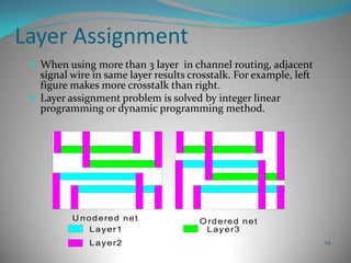
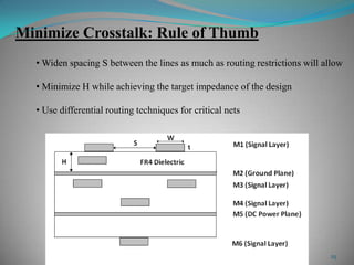
Downloaded 231 times
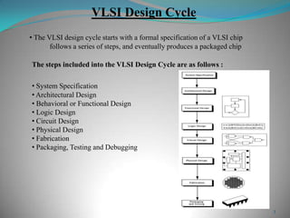
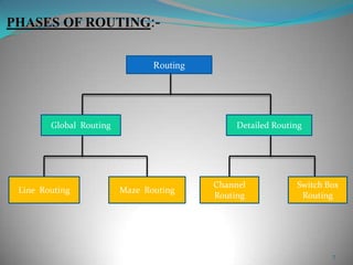
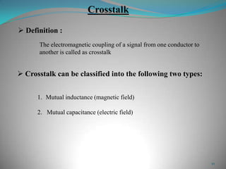
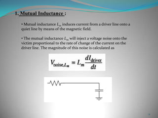
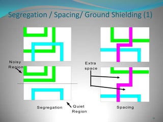
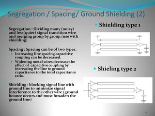
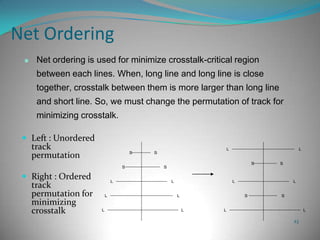


This document summarizes techniques for minimizing crosstalk in VLSI designs. It discusses the VLSI design cycle and physical design cycle. Routing is a key stage that involves global and detailed routing. Crosstalk occurs due to mutual inductance and capacitance between wires and can affect signal integrity, delay, and timing. Basic approaches to reduce crosstalk include segregating wires, increasing spacing between wires, using ground shields, optimizing the net ordering and layer assignments. Specific techniques mentioned are widening spacing, minimizing wire heights and lengths of parallel runs, using differential routing, and routing orthogonal layers.


![Signal Integrity - A Crash Course [R Lott]](https://cdn.slidesharecdn.com/ss_thumbnails/1cb0870c-cad3-4a68-ad41-8e9450fec5d8-170217191645-thumbnail.jpg?width=640&height=640&fit=bounds)


