Downloaded 96 times


![Reduction of Die Size & Power – Doubling Transistor Count
Extending Moore’s law
Reduction of Die Size & Power
IntSim v2.0 free open source >600 downloads
Repeater count increases exponentially with scaling
At 45nm, repeaters >50% of total leakage power of chip [IBM].
Future chip power, area could be dominated by interconnect
repeaters [Saxena P., et al. (Intel), TCAD, 2004]](https://image.slidesharecdn.com/easiestmonolithic3dic-150604062646-lva1-app6892/75/Easiest-Monolithic-3D-IC-39-2048.jpg)


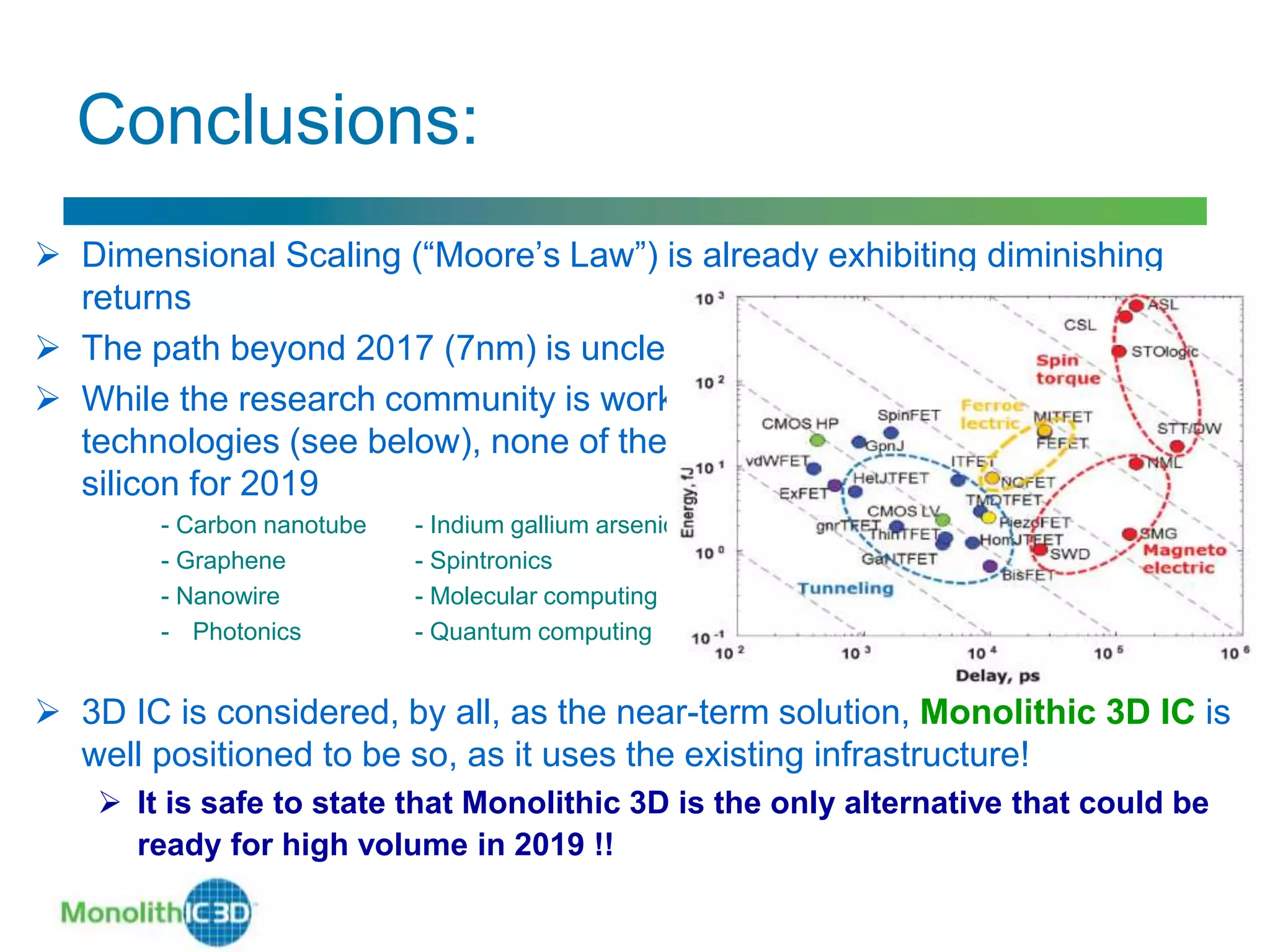
Monolithic 3D IC technology offers a promising solution to the challenges facing traditional 2D ICs, including power consumption and performance limitations, by utilizing existing manufacturing processes. The technology is poised to support further scaling of semiconductor devices, with significant advantages in die size reduction, integration density, and cost. Despite challenges in its widespread adoption, Monolithic 3D IC is considered the most viable alternative for achieving high-volume production by 2019.