Downloaded 66 times
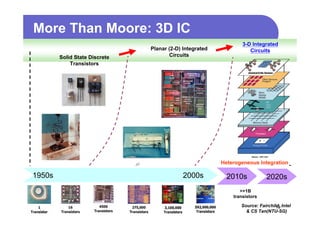
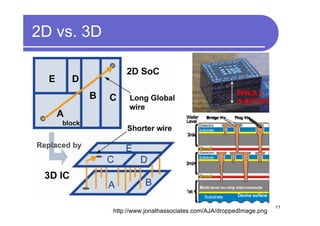
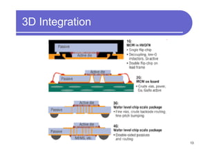
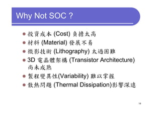

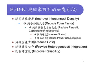
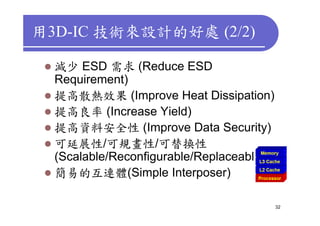
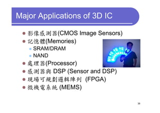
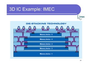
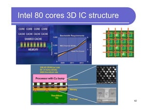
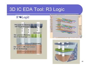
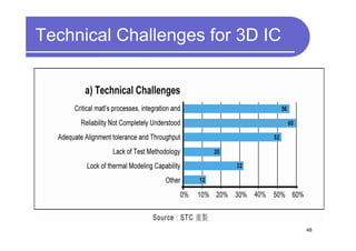


1) 3D IC designs stack multiple silicon dies on top of each other using through-silicon vias (TSVs) to connect the dies. This overcomes limitations of conventional 2D designs like Moore's law. 2) Key advantages of 3D IC include higher density, performance and lower power consumption from shorter interconnects. It also enables heterogeneous integration and improves reliability. 3) Challenges include developing 3D transistor architectures, managing variability and thermal issues across stacked dies, and ensuring design and manufacturing tools are ready to support 3D IC. Major applications are seen in memory, imaging sensors and processors.