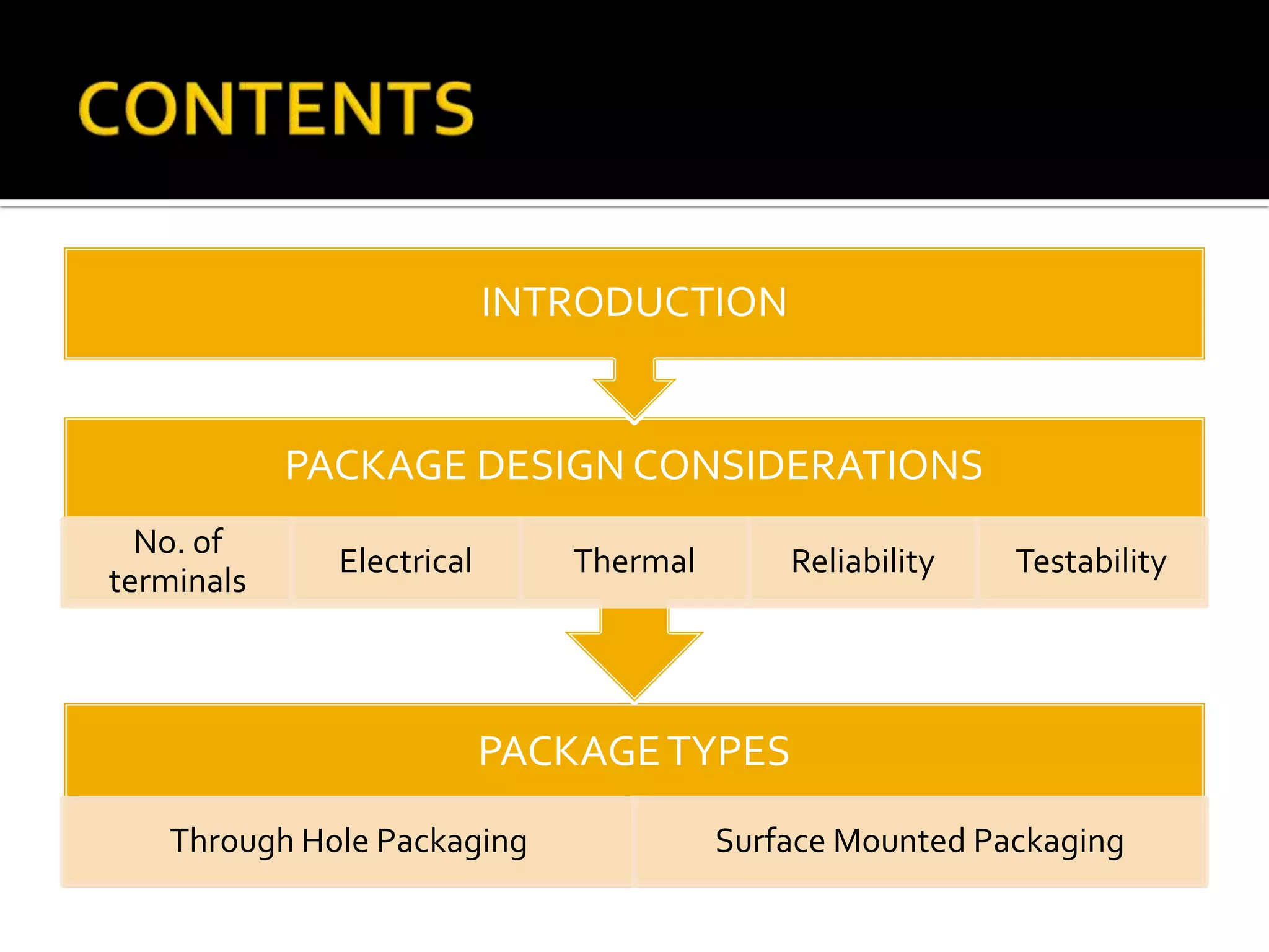
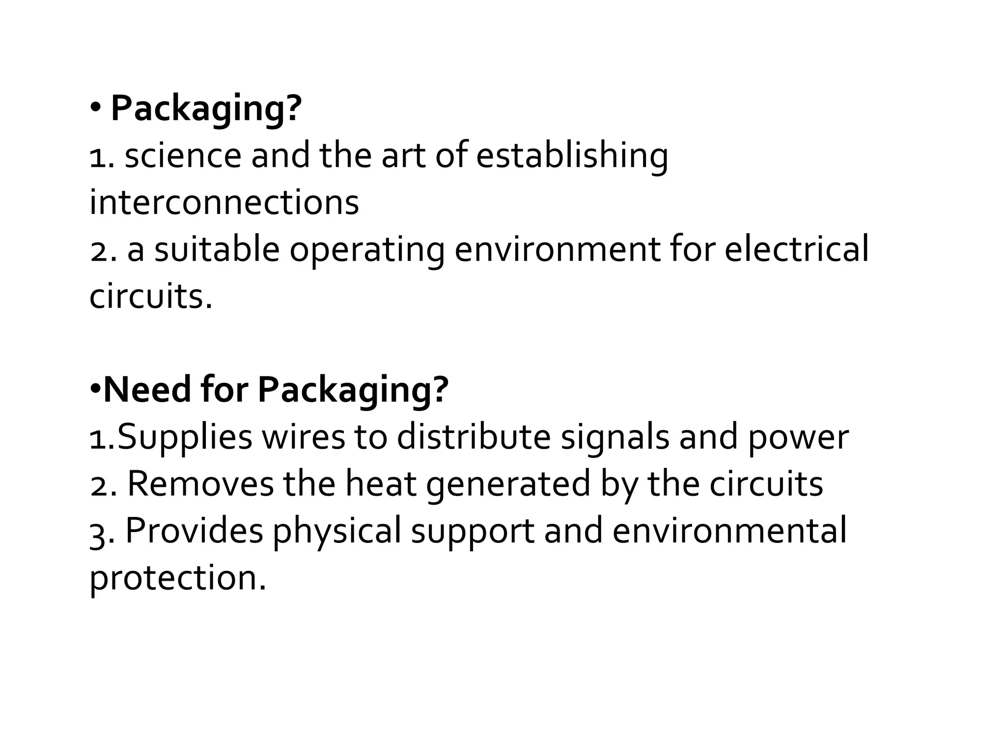
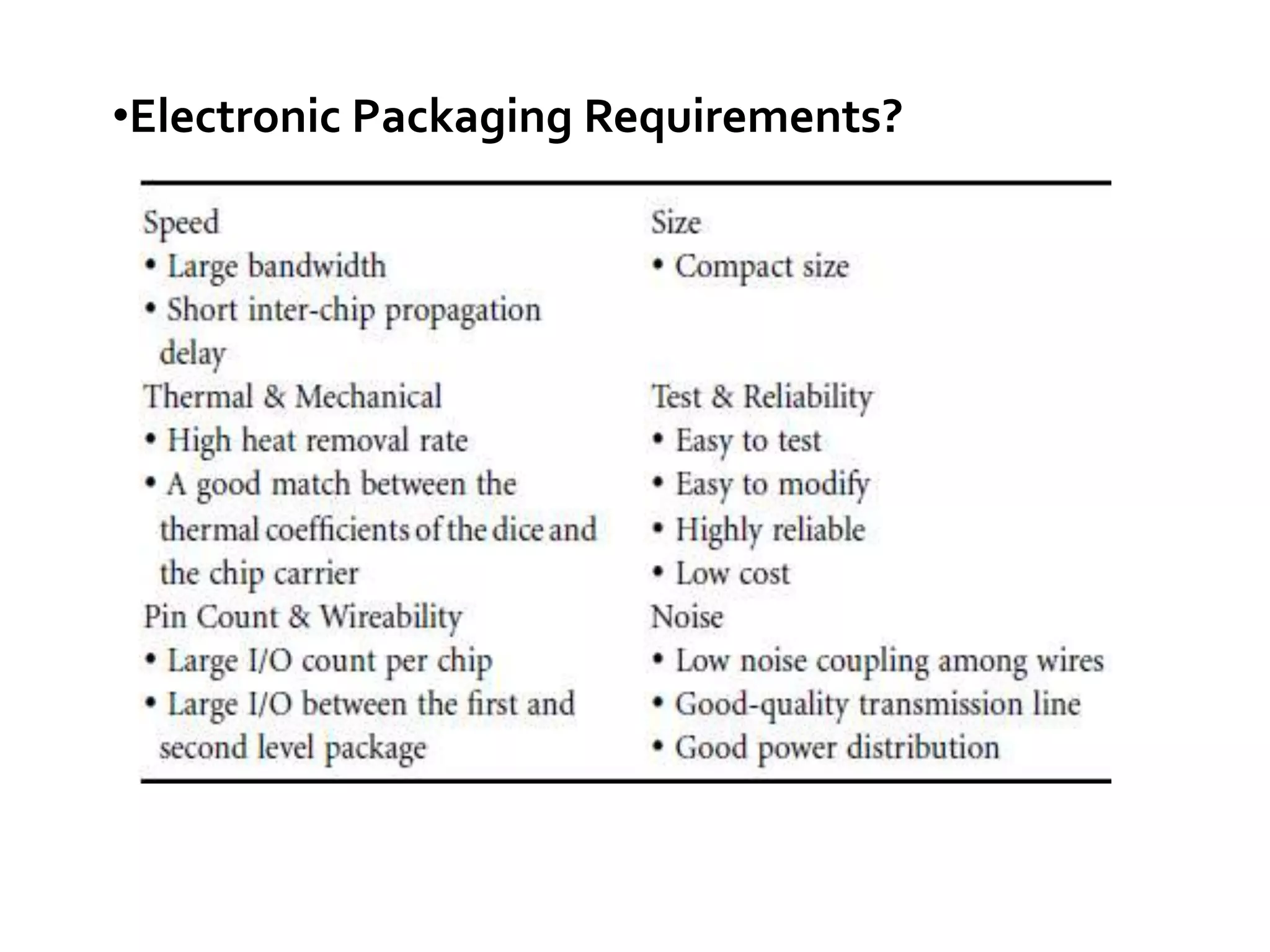
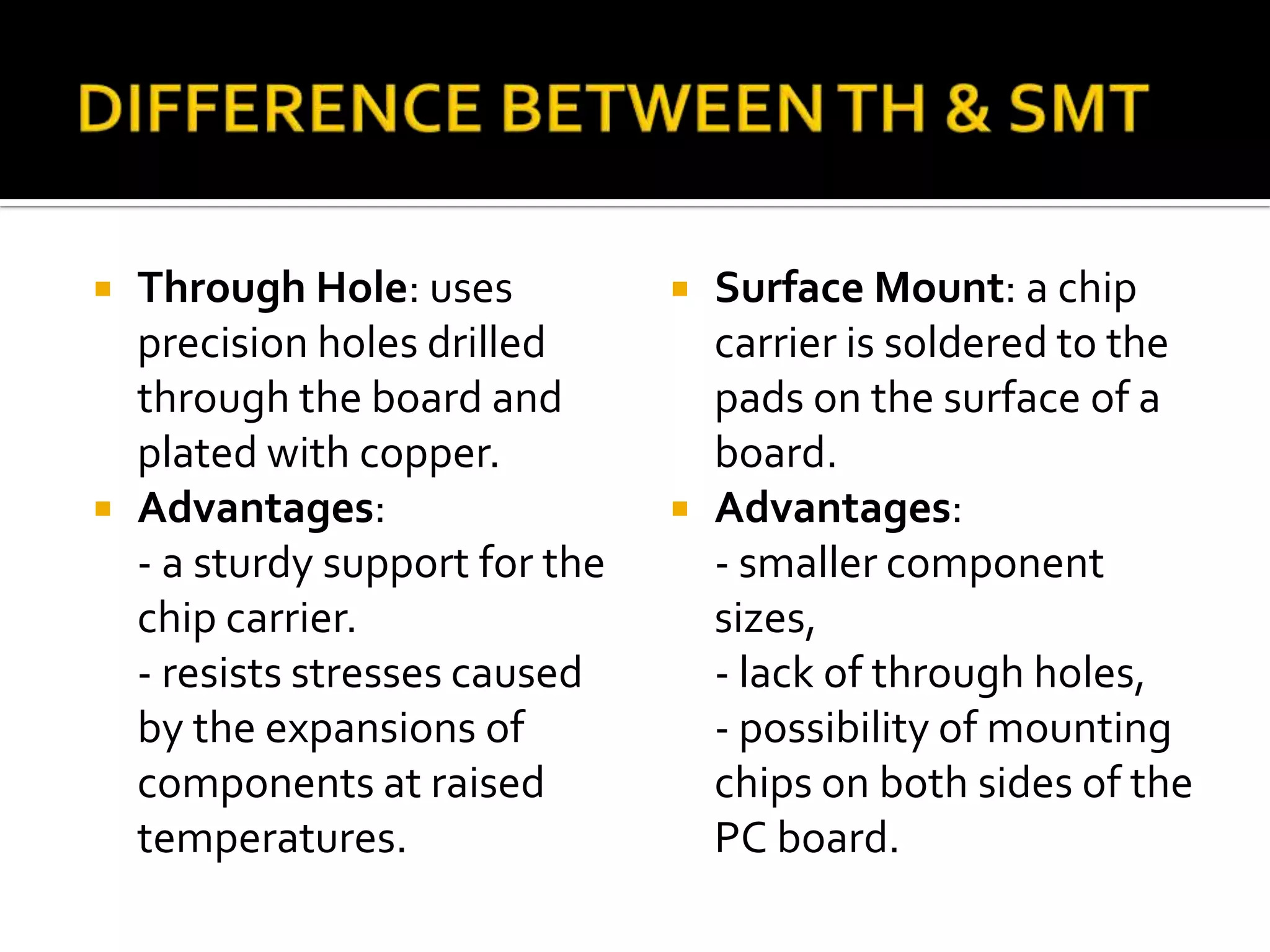
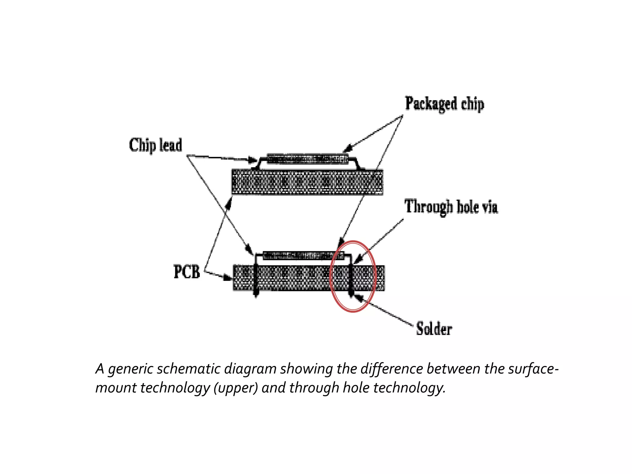
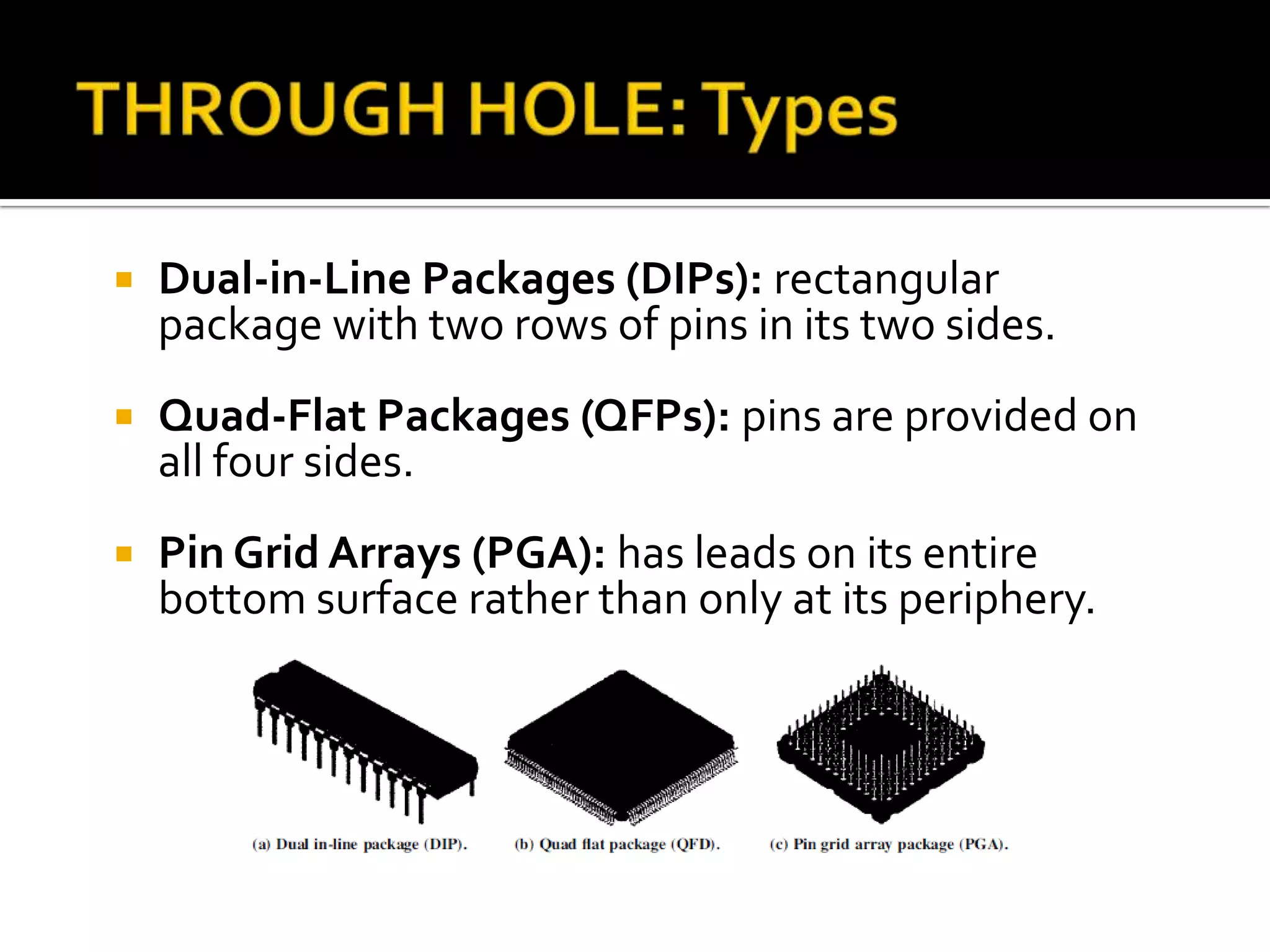
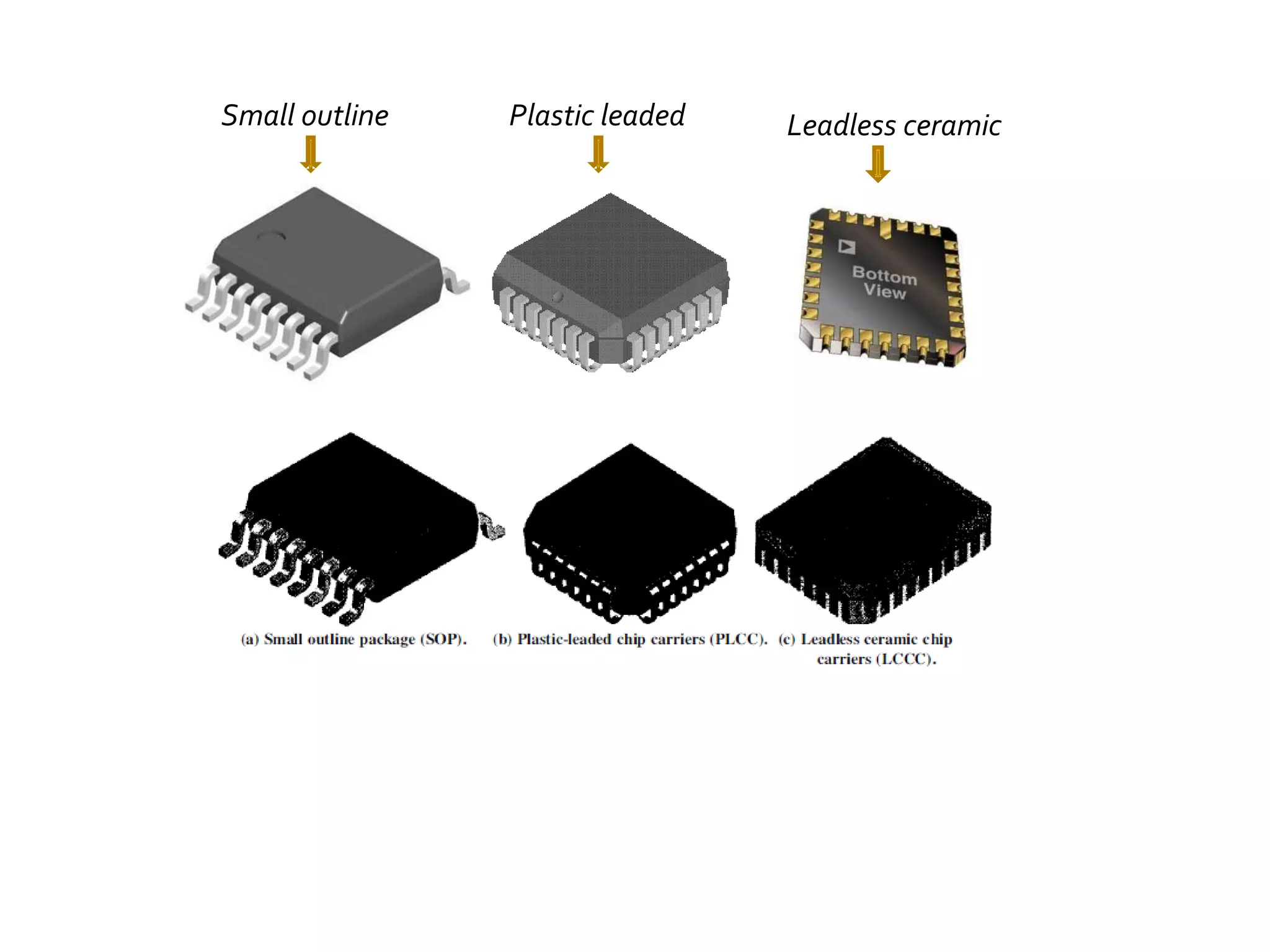
Package Types & Packaging Design Consideration
INTRODUCTION


            PACKAGE DESIGN CONSIDERATIONS
  No. of
              Electrical      Thermal       Reliability   Testability
terminals


                           PACKAGE TYPES
   Through Hole Packaging               Surface Mounted Packaging
•What is packaging?
•What is the need for packaging?
•What are the various packaging requirements?
• Packaging?
1. science and the art of establishing
interconnections
2. a suitable operating environment for electrical
circuits.

•Need for Packaging?
1.Supplies wires to distribute signals and power
2. Removes the heat generated by the circuits
3. Provides physical support and environmental
protection.
•Electronic Packaging Requirements?
•The Basic Rule

•Various Package Parameters
Number of Terminals
Electrical Design Considerations
Thermal Design Considerations
Reliability
Testability
   As a rule, application requirements prescribe:
    1. The number of logic circuits and/or bits of
    storage that must be
    2. packaged (interconnected),
    3. supplied with electric power,
    4. kept within a proper temperature range,
    5. mechanically supported, and
    6. protected against the environment.
1.   No. of Terminals
     - Major cost factor
     - Dependent on the function of VLSI device
     - The smallest pin-out memory IC(stream
     of data can be limited to a single bit)
     - Larger pin-outs  groups of logic
     circuits(result from a random partitioning of
     a computer.)
2.   Electrical Design Considerations
     - As a signal propagates, it is degraded due
     to reflections and line resistance.
     - Controlling the resistance and the
     inductance  Controls switching noise
     - Controlling the impedance  Controls
     reflection-related noise
     - Controlling the capacitive coupling 
     Reduces crosstalk
3.   Thermal Design Considerations:
     - Keep the operating junction temperature
     low prevents triggering the temperature-
     activated failure
     - General recommendation  junction
     temperature < 150°C
     - Heat transfer :
     chip surface (by conduction )
     package surface the ambient (by
     convection and radiation)
4.   Reliability:
     - Good thermo-mechanical performance 
     Good reliability
     - Interfaces are subject to relatively high
     process temperatures as the device is
     powered ON/OFF  residual stresses are
     created  Reliability problems in the
     packages.
5.   Testability:
     - Assumption: a zero defect manufacturing.
     - Rarely practiced because of the high costs.
     - Several tests are employed to assess the
     reliability .
• Basic difference between surface mount(SM) and
through hole(TH) technology
• TH: DIP, QFP and PGA
•SMT: SOP, PLCC and LCCC
• Chip Size Packaging
•Multi Chip Moldules
   Through Hole: uses              Surface Mount: a chip
    precision holes drilled          carrier is soldered to the
    through the board and            pads on the surface of a
    plated with copper.              board.
   Advantages:                     Advantages:
    - a sturdy support for the       - smaller component
    chip carrier.                    sizes,
    - resists stresses caused        - lack of through holes,
    by the expansions of             - possibility of mounting
    components at raised             chips on both sides of the
    temperatures.                    PC board.
A generic schematic diagram showing the difference between the surface-
mount technology (upper) and through hole technology.
   Dual-in-Line Packages (DIPs): rectangular
    package with two rows of pins in its two sides.
   Quad-Flat Packages (QFPs): pins are provided on
    all four sides.
   Pin Grid Arrays (PGA): has leads on its entire
    bottom surface rather than only at its periphery.
   Small-Outline Packages (SOPs): has gull-wing
    shaped leads;
    Advantage: requires less pin spacing
   Plastic-leaded chip carriers(PLCCs):
    Advantage: offer higher pin counts than SOP as
    J-leaded chip carriers pack denser.
   Leadless Ceramic Chip Carriers (LCCCs): The
    conductors are left exposed around the package;
    Advantage: Uses multilayer ceramic technology
    which has high thermal conductivity.
Small outline   Plastic leaded   Leadless ceramic
Packaging of vlsi devices

Packaging of vlsi devices

  • 1.
    Package Types &Packaging Design Consideration
  • 2.
    INTRODUCTION PACKAGE DESIGN CONSIDERATIONS No. of Electrical Thermal Reliability Testability terminals PACKAGE TYPES Through Hole Packaging Surface Mounted Packaging
  • 3.
    •What is packaging? •Whatis the need for packaging? •What are the various packaging requirements?
  • 4.
    • Packaging? 1. scienceand the art of establishing interconnections 2. a suitable operating environment for electrical circuits. •Need for Packaging? 1.Supplies wires to distribute signals and power 2. Removes the heat generated by the circuits 3. Provides physical support and environmental protection.
  • 5.
  • 6.
    •The Basic Rule •VariousPackage Parameters Number of Terminals Electrical Design Considerations Thermal Design Considerations Reliability Testability
  • 7.
    As a rule, application requirements prescribe: 1. The number of logic circuits and/or bits of storage that must be 2. packaged (interconnected), 3. supplied with electric power, 4. kept within a proper temperature range, 5. mechanically supported, and 6. protected against the environment.
  • 8.
    1. No. of Terminals - Major cost factor - Dependent on the function of VLSI device - The smallest pin-out memory IC(stream of data can be limited to a single bit) - Larger pin-outs  groups of logic circuits(result from a random partitioning of a computer.)
  • 9.
    2. Electrical Design Considerations - As a signal propagates, it is degraded due to reflections and line resistance. - Controlling the resistance and the inductance  Controls switching noise - Controlling the impedance  Controls reflection-related noise - Controlling the capacitive coupling  Reduces crosstalk
  • 10.
    3. Thermal Design Considerations: - Keep the operating junction temperature low prevents triggering the temperature- activated failure - General recommendation  junction temperature < 150°C - Heat transfer : chip surface (by conduction ) package surface the ambient (by convection and radiation)
  • 11.
    4. Reliability: - Good thermo-mechanical performance  Good reliability - Interfaces are subject to relatively high process temperatures as the device is powered ON/OFF  residual stresses are created  Reliability problems in the packages.
  • 12.
    5. Testability: - Assumption: a zero defect manufacturing. - Rarely practiced because of the high costs. - Several tests are employed to assess the reliability .
  • 13.
    • Basic differencebetween surface mount(SM) and through hole(TH) technology • TH: DIP, QFP and PGA •SMT: SOP, PLCC and LCCC • Chip Size Packaging •Multi Chip Moldules
  • 14.
    Through Hole: uses  Surface Mount: a chip precision holes drilled carrier is soldered to the through the board and pads on the surface of a plated with copper. board.  Advantages:  Advantages: - a sturdy support for the - smaller component chip carrier. sizes, - resists stresses caused - lack of through holes, by the expansions of - possibility of mounting components at raised chips on both sides of the temperatures. PC board.
  • 15.
    A generic schematicdiagram showing the difference between the surface- mount technology (upper) and through hole technology.
  • 16.
    Dual-in-Line Packages (DIPs): rectangular package with two rows of pins in its two sides.  Quad-Flat Packages (QFPs): pins are provided on all four sides.  Pin Grid Arrays (PGA): has leads on its entire bottom surface rather than only at its periphery.
  • 17.
    Small-Outline Packages (SOPs): has gull-wing shaped leads; Advantage: requires less pin spacing  Plastic-leaded chip carriers(PLCCs): Advantage: offer higher pin counts than SOP as J-leaded chip carriers pack denser.  Leadless Ceramic Chip Carriers (LCCCs): The conductors are left exposed around the package; Advantage: Uses multilayer ceramic technology which has high thermal conductivity.
  • 18.
    Small outline Plastic leaded Leadless ceramic