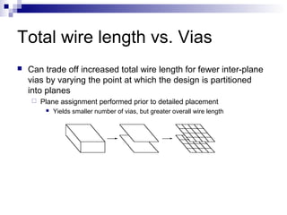
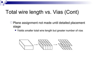
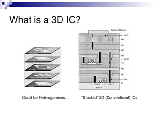
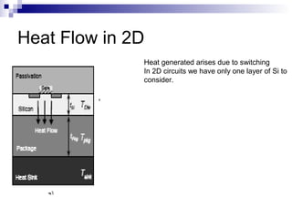
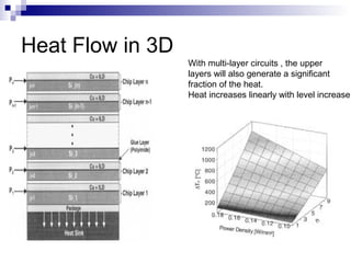
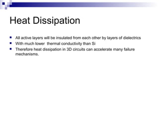
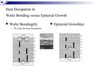
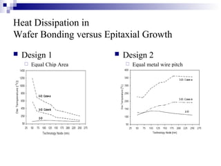
3D IC technology

Pouya Dormiani
Christopher Lucas
What is a 3D IC?


  Could be Heterogeneous…   “Stacked” 2D (Conventional) ICs
Motivation
   Interconnect structures increasingly consume more of the power
    and delay budgets in modern design
   Plausible solution: increase the number of “nearest neighbors” seen
    by each transistor by using 3D IC design
   Smaller wire cross-sections, smaller wire pitch and longer lines to
    traverse larger chips increase RC delay.
        RC delay is increasingly becoming the dominant factor
   At 250 nm Cu was introduced alleviate the adverse effect of
    increasing interconnect delay.
    130 nm technology node, substantial interconnect delays will result.
3D Fabrication Technologies
        Many options available for realization of 3D circuits
        Choice of Fabrication depends on requirements of
         Circuit System
Beam                            Processed Wafer                  Silicon Epitaxial                Solid Phase
Recrystallization               Bonding                          Growth                           Crystallization

Deposit polysillicon            Bond two fully                   Epitaxially grow a               Low Temp
and fabricate TFTs              processed wafers                 single cystal Si                 alternative to SE.
-not practial for 3D circuits   together.
due to high temp of melting
polysillicon
                                -Similar Electrical Properties   -High temperatures cause         -Offers Flexibilty of creating
                                on all devices                   siginificant cause significant   multiple layers
-Suffers from Low carrier
                                -Independent of temp. since      degradation in quality of        -Compatible with current
mobility
                                all chips are fabricated then    devices on lower layers          processing environments
-However high perfomance        bonded
TFT’s                                                            -Process not yet                 -Useful for Stacked SRAM
                                -Good for applications where     manufacturable                   and EEPROM cells
have been fabricated using      chips do independent
low temp processing which       processing
can be used to implement 3D
                                -However Lack of
circuits
                                Precision(alignemnt) restricts
                                interchip communication to
                                global metal lines.
Performance Characteristics
 Timing
 Energy
   With shorter interconnects in 3D ICs, both switching
    energy and cycle time are expected to be reduced
Timing
   In current technologies, timing is
    interconnect driven.
   Reducing interconnect length in
    designs can dramatically reduce
    RC delays and increase chip
    performance
   The graph below shows the
    results of a reduction in wire
    length due to 3D routing
   Discussed more in detail later in
    the slides
Energy performance
 Wire length reduction has an impact on
  the cycle time and the energy dissipation
 Energy dissipation decreases with the
  number of layers used in the design
 Following graphs are based on the 3D tool
  described later in the presentation
Energy performance graphs
Design tools for 3D-IC design
   Demand for EDA tools
     Asthe technology matures, designers will
      want to exploit this design area
   Current tool-chains
     Mostly    academic
          We will discuss a tool from MIT
3D Standard Cell tool Design
   3D Cell Placement
     Placement     by min-cut partitioning
   3D Global Routing
     Inter-wafer   vias
   Circuit layout management
     MAGIC
3D Standard Cell Placement
   Natural to think of a 3D
    integrated circuit as
    being partitioned into
    device layers or planes
   Min cut part-itioning
    along the 3rd dimension
    is same as minimizing
    vias
Total wire length vs. Vias
   Can trade off increased total wire length for fewer inter-plane
    vias by varying the point at which the design is partitioned
    into planes
       Plane assignment performed prior to detailed placement
            Yields smaller number of vias, but greater overall wire length
Total wire length vs. Vias (Cont)
   Plane    assignment not made until detailed placement
   stage
        Yields smaller total wire length but greater number of vias
Intro to Global Routing
   Overview
     Global Routing involves generating a “loose”
     route for each net.
         Assigns a list of routing regions to a net without
          actually specifying the geometrical layout of the
          wires.
     Followed    by detailed routing
         Finds the actual geometrical shape of the net
          within the assigned routing regions.
     Usuallyeither sequential or hierarchical
     algorithms
Illustration of routing areas

               y                            y


  x                   x


           z                           z


                   Detailed routing of net when
                   routing areas are known
Hierarchical Global Routing
   Tool uses a hierarchical global routing
    algorithm
     Based   on Integer programming and Steiner
      trees
     Integer programming approach still too slow
      for size of problem and complexity (NP-hard)
     Hierarchical routing methods break down the
      integer program into pieces small enough to
      be solved exactly
2D Global Routing
   A 2D Hierarchical global router works by recursively
    bisecting the routing substrate.
       Wires within a Region are fully contained or terminate at a
        pin on the region boundry.
   At each partitioning step the pins on the side of the
    routing region is allocated to one of the two subregions.
   Wires Connect cells on both sides of the partition line.
       These are cut by the partition and for each a pin is inserted
        into the side of the partition
   Once complete, the results can be fed to a detailed
    router or switch box router (A switchbox is a rectangular
    area bounded on all sides by blocks)
Illustration of Bisection
Extending to 3D
   Routing in 3D consists of routing a set of aligned
    congruent routing regions on adjacent wafers.
       Wires can enter from any of the sides of the routing region in
        addition to its top and bottom
   3D router must consider routing on each of the layers in
    addition to the placement of the inter-waver vias
   Basis idea is: You connect a inter-waver via to the port
    you are trying to connect to, and route the wire to that via
    on the 2D plane.
       All we need now is enough area in the 2D routing space to route
        to the appropriate via
3D Routing Results
                     Percentage Of 2D
                     Total wire Length
                     Minimizing for Wire Length:
                     2 Layers ~ 28%
                     5 Layers ~ 51 %


                     Minimizing for via count:
                     2 Layers ~ 7%
                     5 Layers ~ 17%
3D-MAGIC
   MAGIC is an open source layout editor developed at UC
    Berkeley
   3D-MAGIC is an extension to MAGIC by providing
    support for Multi-layer IC design
   What’s different
     New Command :bond
     Bonds existing 2D ICs and places inter-layer Vias in the design
      file
     Once Two layers are bonded they are treated as one entity
Concerns in 3D circuit
 Thermal Issues in 3D-circuits
 EMI
 Reliability Issues
Thermal Issues in 3D Circuits

   Thermal Effects dramatically impact interconnect and device reliability in 2D
    circuits
   Due to reduction in chip size of a 3D implementation, 3D circuits exhibit a sharp
    increase in power density
   Analysis of Thermal problems in 3D is necessary to evaluate thermal robustness of
    different 3D technology and design options.
Heat Flow in 2D
              Heat generated arises due to switching
              In 2D circuits we have only one layer of Si to
              consider.
Heat Flow in 3D
                  With multi-layer circuits , the upper
                  layers will also generate a significant
                  fraction of the heat.
                  Heat increases linearly with level increase
Heat Dissipation
   All active layers will be insulated from each other by layers of dielectrics
   With much lower thermal conductivity than Si
   Therefore heat dissipation in 3D circuits can accelerate many failure
    mechanisms.
Heat Dissipation in
Wafer Bonding versus Epitaxial Growth

   Wafer Bonding(b)                      Epitaxial Growth(a)
       2X Area for heat dissipation
Heat Dissipation in
Wafer Bonding versus Epitaxial Growth
   Design 1                 Design 2
       Equal Chip Area          Equal metal wire pitch
High epitaxial temperature
          Temperatures actually higher for Epitaxial second layers
          Since the temperature of the second active layer T2 will
          Be higher than T1 since T1 is closer to the substrate
          and T2 is stuck between insulators
EMI in 3D ICs
   Interconnect Coupling Capacitance and cross talk
        Coupling between the top layer metal of the first active layer and the device on
         the second active layer devices is expected
EMI
   Interconnect Inductance Effects
     Shorter wire lengths help reduce the
      inductance
     Presence of second substrate close to global
      wires might help lower inductance by
      providing shorter return paths
Reliability Issues?
   Electro thermal and Thermo-mechanical effects
    between various active layers can influence electro-
    migration and chip performance
   Die yield issues may arise due to mismatches
    between die yields of different layers, which affect
    net yield of 3D chips.
Implications on Circuit Design
and Architecture

   Buffer Insertion
   Layout of Critical Paths
   Microprocessor Design
   Mixed Signal IC’s
   Physical design and Synthesis
Buffer Insertion

   Buffer Insertion
     Use of buffers in 3D circuits to break up long interconnects
     At top layers inverter sizes 450 times min inverter size for the relevant
      technology
     These top layer buffers require large routing area and can reach up to
      10,000 for high performance designs in 100nm technology
     With 3D technology repeaters can be placed on the second layer and
      reduce area for the first layer.
Layout of Critical Paths and
Microprocessor Design
   Once again interconnect delay dominates in 2D
    design.
   Logic blocks on the critical path need to
    communicate with each other but due to
    placement and desig constraints are placed far
    away from each other.
   With a second layer of Si these devices can be
    placed on different layes of Si and thus closer to
    each other using(VILICs)

   In Microprocessor design most critical paths
    involve on chip caches on the critical path.
   Computational modules which access the cache
    are distributed all over the chip while the cache
    is in the corner.
   Cache can be placed on a second layer and
    connected to these modules using (VILICs)
Mixed Signal ICs and Physical
Design
   Digital signals on chip can couple and interfere with
    RF signals
   With multiple layers RF portions of the system can be
    separated from their digital counterparts.
   Physical Design needs to consider the multiple layers
    of Silicon available.
   Placement and routing algorithms need to be
    modified
Conclusion
 3D IC design is a relief to interconnect
  driven IC design.
 Still many manufacturing and
  technological difficulties
 Needs strong EDA applications for
  automated design

3 d

  • 1.
    3D IC technology PouyaDormiani Christopher Lucas
  • 2.
    What is a3D IC? Could be Heterogeneous… “Stacked” 2D (Conventional) ICs
  • 3.
    Motivation  Interconnect structures increasingly consume more of the power and delay budgets in modern design  Plausible solution: increase the number of “nearest neighbors” seen by each transistor by using 3D IC design  Smaller wire cross-sections, smaller wire pitch and longer lines to traverse larger chips increase RC delay.  RC delay is increasingly becoming the dominant factor  At 250 nm Cu was introduced alleviate the adverse effect of increasing interconnect delay.  130 nm technology node, substantial interconnect delays will result.
  • 4.
    3D Fabrication Technologies  Many options available for realization of 3D circuits  Choice of Fabrication depends on requirements of Circuit System Beam Processed Wafer Silicon Epitaxial Solid Phase Recrystallization Bonding Growth Crystallization Deposit polysillicon Bond two fully Epitaxially grow a Low Temp and fabricate TFTs processed wafers single cystal Si alternative to SE. -not practial for 3D circuits together. due to high temp of melting polysillicon -Similar Electrical Properties -High temperatures cause -Offers Flexibilty of creating on all devices siginificant cause significant multiple layers -Suffers from Low carrier -Independent of temp. since degradation in quality of -Compatible with current mobility all chips are fabricated then devices on lower layers processing environments -However high perfomance bonded TFT’s -Process not yet -Useful for Stacked SRAM -Good for applications where manufacturable and EEPROM cells have been fabricated using chips do independent low temp processing which processing can be used to implement 3D -However Lack of circuits Precision(alignemnt) restricts interchip communication to global metal lines.
  • 5.
    Performance Characteristics  Timing Energy  With shorter interconnects in 3D ICs, both switching energy and cycle time are expected to be reduced
  • 6.
    Timing  In current technologies, timing is interconnect driven.  Reducing interconnect length in designs can dramatically reduce RC delays and increase chip performance  The graph below shows the results of a reduction in wire length due to 3D routing  Discussed more in detail later in the slides
  • 7.
    Energy performance  Wirelength reduction has an impact on the cycle time and the energy dissipation  Energy dissipation decreases with the number of layers used in the design  Following graphs are based on the 3D tool described later in the presentation
  • 8.
  • 9.
    Design tools for3D-IC design  Demand for EDA tools  Asthe technology matures, designers will want to exploit this design area  Current tool-chains  Mostly academic  We will discuss a tool from MIT
  • 10.
    3D Standard Celltool Design  3D Cell Placement  Placement by min-cut partitioning  3D Global Routing  Inter-wafer vias  Circuit layout management  MAGIC
  • 11.
    3D Standard CellPlacement  Natural to think of a 3D integrated circuit as being partitioned into device layers or planes  Min cut part-itioning along the 3rd dimension is same as minimizing vias
  • 12.
    Total wire lengthvs. Vias  Can trade off increased total wire length for fewer inter-plane vias by varying the point at which the design is partitioned into planes  Plane assignment performed prior to detailed placement  Yields smaller number of vias, but greater overall wire length
  • 13.
    Total wire lengthvs. Vias (Cont)  Plane assignment not made until detailed placement stage  Yields smaller total wire length but greater number of vias
  • 14.
    Intro to GlobalRouting  Overview  Global Routing involves generating a “loose” route for each net.  Assigns a list of routing regions to a net without actually specifying the geometrical layout of the wires.  Followed by detailed routing  Finds the actual geometrical shape of the net within the assigned routing regions.  Usuallyeither sequential or hierarchical algorithms
  • 15.
    Illustration of routingareas y y x x z z Detailed routing of net when routing areas are known
  • 16.
    Hierarchical Global Routing  Tool uses a hierarchical global routing algorithm  Based on Integer programming and Steiner trees  Integer programming approach still too slow for size of problem and complexity (NP-hard)  Hierarchical routing methods break down the integer program into pieces small enough to be solved exactly
  • 17.
    2D Global Routing  A 2D Hierarchical global router works by recursively bisecting the routing substrate.  Wires within a Region are fully contained or terminate at a pin on the region boundry.  At each partitioning step the pins on the side of the routing region is allocated to one of the two subregions.  Wires Connect cells on both sides of the partition line.  These are cut by the partition and for each a pin is inserted into the side of the partition  Once complete, the results can be fed to a detailed router or switch box router (A switchbox is a rectangular area bounded on all sides by blocks)
  • 18.
  • 19.
    Extending to 3D  Routing in 3D consists of routing a set of aligned congruent routing regions on adjacent wafers.  Wires can enter from any of the sides of the routing region in addition to its top and bottom  3D router must consider routing on each of the layers in addition to the placement of the inter-waver vias  Basis idea is: You connect a inter-waver via to the port you are trying to connect to, and route the wire to that via on the 2D plane.  All we need now is enough area in the 2D routing space to route to the appropriate via
  • 20.
    3D Routing Results Percentage Of 2D Total wire Length Minimizing for Wire Length: 2 Layers ~ 28% 5 Layers ~ 51 % Minimizing for via count: 2 Layers ~ 7% 5 Layers ~ 17%
  • 21.
    3D-MAGIC  MAGIC is an open source layout editor developed at UC Berkeley  3D-MAGIC is an extension to MAGIC by providing support for Multi-layer IC design  What’s different  New Command :bond  Bonds existing 2D ICs and places inter-layer Vias in the design file  Once Two layers are bonded they are treated as one entity
  • 22.
    Concerns in 3Dcircuit  Thermal Issues in 3D-circuits  EMI  Reliability Issues
  • 23.
    Thermal Issues in3D Circuits  Thermal Effects dramatically impact interconnect and device reliability in 2D circuits  Due to reduction in chip size of a 3D implementation, 3D circuits exhibit a sharp increase in power density  Analysis of Thermal problems in 3D is necessary to evaluate thermal robustness of different 3D technology and design options.
  • 24.
    Heat Flow in2D Heat generated arises due to switching In 2D circuits we have only one layer of Si to consider.
  • 25.
    Heat Flow in3D With multi-layer circuits , the upper layers will also generate a significant fraction of the heat. Heat increases linearly with level increase
  • 26.
    Heat Dissipation  All active layers will be insulated from each other by layers of dielectrics  With much lower thermal conductivity than Si  Therefore heat dissipation in 3D circuits can accelerate many failure mechanisms.
  • 27.
    Heat Dissipation in WaferBonding versus Epitaxial Growth  Wafer Bonding(b)  Epitaxial Growth(a)  2X Area for heat dissipation
  • 28.
    Heat Dissipation in WaferBonding versus Epitaxial Growth  Design 1  Design 2  Equal Chip Area  Equal metal wire pitch
  • 29.
    High epitaxial temperature Temperatures actually higher for Epitaxial second layers Since the temperature of the second active layer T2 will Be higher than T1 since T1 is closer to the substrate and T2 is stuck between insulators
  • 30.
    EMI in 3DICs  Interconnect Coupling Capacitance and cross talk  Coupling between the top layer metal of the first active layer and the device on the second active layer devices is expected
  • 31.
    EMI  Interconnect Inductance Effects  Shorter wire lengths help reduce the inductance  Presence of second substrate close to global wires might help lower inductance by providing shorter return paths
  • 32.
    Reliability Issues?  Electro thermal and Thermo-mechanical effects between various active layers can influence electro- migration and chip performance  Die yield issues may arise due to mismatches between die yields of different layers, which affect net yield of 3D chips.
  • 33.
    Implications on CircuitDesign and Architecture  Buffer Insertion  Layout of Critical Paths  Microprocessor Design  Mixed Signal IC’s  Physical design and Synthesis
  • 34.
    Buffer Insertion  Buffer Insertion  Use of buffers in 3D circuits to break up long interconnects  At top layers inverter sizes 450 times min inverter size for the relevant technology  These top layer buffers require large routing area and can reach up to 10,000 for high performance designs in 100nm technology  With 3D technology repeaters can be placed on the second layer and reduce area for the first layer.
  • 35.
    Layout of CriticalPaths and Microprocessor Design  Once again interconnect delay dominates in 2D design.  Logic blocks on the critical path need to communicate with each other but due to placement and desig constraints are placed far away from each other.  With a second layer of Si these devices can be placed on different layes of Si and thus closer to each other using(VILICs)  In Microprocessor design most critical paths involve on chip caches on the critical path.  Computational modules which access the cache are distributed all over the chip while the cache is in the corner.  Cache can be placed on a second layer and connected to these modules using (VILICs)
  • 36.
    Mixed Signal ICsand Physical Design  Digital signals on chip can couple and interfere with RF signals  With multiple layers RF portions of the system can be separated from their digital counterparts.  Physical Design needs to consider the multiple layers of Silicon available.  Placement and routing algorithms need to be modified
  • 37.
    Conclusion  3D ICdesign is a relief to interconnect driven IC design.  Still many manufacturing and technological difficulties  Needs strong EDA applications for automated design