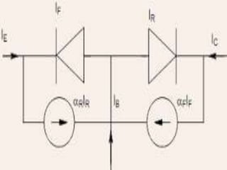
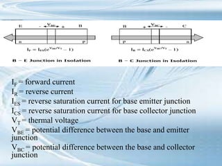
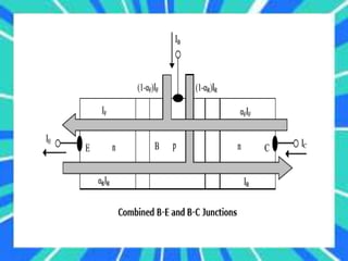
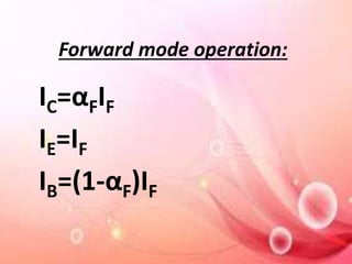
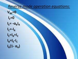
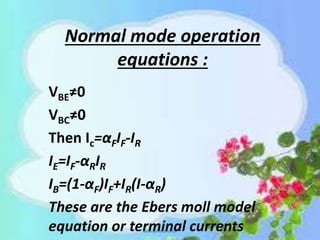
The document discusses MOSFETs (metal-oxide-semiconductor field-effect transistors). It provides information on:
1) The structure of MOSFETs including typical dimensions of the gate length and width. It operates by using a voltage applied to the gate to control the conductivity between the drain and source.
2) The operation of n-channel and p-channel MOSFETs. In an n-channel MOSFET, applying a positive voltage to the gate creates an n-type inversion channel between the source and drain allowing current to flow.
3) Biasing techniques for MOSFET amplifiers including fixing the gate voltage, connecting a resistor in the source,
There are four main methods of transistor biasing: base resistor method, emitter bias method, biasing with collector feedback resistor, and voltage-divider bias method. The document then focuses on explaining the base resistor method and voltage-divider bias method in more detail. For the base resistor method, a resistor is used to provide base current, but it has poor stability. For the voltage-divider bias method, two resistors are used to provide stable biasing of the transistor by controlling the base-emitter voltage. This method is widely used due to its stability from the emitter resistor preventing changes in collector current.
This document provides an overview of the Junction Field Effect Transistor (JFET). It discusses the construction of JFETs including the source, drain and gate terminals. It describes the theory of operation explaining how applying voltages to the gate can control the channel and current flow. The key sections outline the characteristic I-V curve, pinch-off voltage, saturation level and cut-off voltage. Advantages of JFETs are also summarized such as high input impedance. Common applications are listed including use as amplifiers and constant current sources.
This document discusses MOSFETs and JFETs. It introduces MOSFETs, describing the metal oxide layer and how the electric field controls current. It describes types of MOSFETs and their applications, particularly as switches. Characteristic curves of MOSFETs are also mentioned. The document then introduces JFETs, describing their structure and operation. Applications of JFETs as switches are provided. Advantages and disadvantages of JFETs are listed. Finally, characteristics curves of JFETs, including output and transfer characteristics, are described.
- The JFET is a voltage-controlled device that uses an electric field to control the flow of current. It has three terminals: the drain, gate, and source.
- There are two types of JFETs: n-channel and p-channel. In an n-channel JFET, applying a negative voltage to the gate reduces the channel width and thereby the current between the drain and source. In a p-channel JFET the behavior is opposite.
- The JFET characteristics show the drain current (ID) as a function of drain-source voltage (VDS) for different gate-source voltages (VGS). ID increases with VDS until reaching pinch-off, then becomes constant.
The MOSFET is an important element in embedded system design which is used to control the loads as per the requirement. The MOSFET is a high voltage controlling device provides some key features for circuit designers in terms of their overall performance.
The three terminals of the FET are known as Gate, Drain, and Source.
It is a voltage controlled device, where the input voltage controls by the output current.
In FET current used to flow between the drain and the source terminal. And this current can be controlled by applying the voltage between the gate and the source terminal.
So this applied voltage generate the electric field within the device and by controlling these electric field we can control the flow of current through the device.
Mosfet
MOSFETs have characteristics similar to JFETs and additional characteristics that make them very useful.
There are 2 types:
• Depletion-Type MOSFET
• Enhancement-Type MOSFET
The document discusses the bipolar junction transistor (BJT). It describes how the BJT was invented in 1947 by scientists at Bell Labs. The BJT consists of three terminals - the emitter, base, and collector - and comes in two types, p-n-p and n-p-n. The document explains the basic operation and principles of both types of BJT, including how current flows when junctions are forward or reverse biased in different modes. It also provides examples of calculating currents given bias conditions and current gains. Finally, it summarizes the key current-voltage relationships and characteristics of BJTs in common base, common emitter, and common collector configurations.
This document discusses different digital logic families and characteristics. It describes Resistor-Transistor Logic (RTL) which consists of resistors and transistors, with the emitters connected to ground and collectors tied through a resistor. Transistor-Transistor Logic (TTL) is also discussed, which depends solely on transistors. TTL uses multiple emitter transistors for inputs and a totem-pole output for high speed and low impedance. The document provides details on RTL and TTL gate operations.
A MOSFET is a semiconductor device that can amplify or switch electronic signals. It has three terminals - drain, source, and gate. Depending on whether the semiconductor material between the drain and source is n-type or p-type, a MOSFET can be an n-channel or p-channel type. Applying a positive voltage to the gate of an n-channel MOSFET or a negative voltage to the gate of a p-channel MOSFET allows current to flow between the drain and source. MOSFETs are commonly used as switches in digital circuits like processors and as amplifiers in analog circuits. They are also used in memory devices, power supplies, and other electronic applications.
The MOSFET is a four-terminal semiconductor device used for switching and amplifying electronic signals. It comes in two basic forms, P-channel and N-channel, and two modes, depletion and enhancement. MOSFETs exhibit three operating regions - cut-off, where no current flows; ohmic or linear, where current increases with drain-source voltage; and saturation, where current reaches a maximum. MOSFETs are voltage-controlled, unipolar devices that can switch or amplify depending on their operating region.
The document discusses different types of field effect transistors (FETs), including junction FETs (JFETs), metal-oxide-semiconductor FETs (MOSFETs), and metal-semiconductor FETs (MESFETs). It focuses on the structure and operation of n-channel and p-channel MOSFETs, describing how a positive or negative gate voltage is used to create a conducting channel. Scaling challenges for MOSFETs are also discussed, along with new materials needed like high-k dielectrics and metal gates, and approaches like silicon-on-insulator (SOI) technology.
This document presents an overview of operational amplifiers (op-amps). It begins with an introduction to op-amps, followed by their circuit symbol, pin diagram, important terms and equations. It describes the ideal properties of an op-amp, as well as non-ideal behaviors. Applications discussed include analog to digital converters, current sources, and zero crossing detectors. Advantages are listed as versatility and uses in various circuits. Disadvantages include limitations in power and load resistance.
This document provides an introduction to transistors and MOSFETs. It begins by describing the invention of the transistor in 1947 and defining what a transistor is. It then discusses the main types of transistors - BJT and FET, including MOSFET and JFET. The rest of the document focuses on MOSFETs, explaining what they are, their terminals and symbols, types of MOSFETs like n-MOSFET and p-MOSFET, and how MOSFETs work and are fabricated through processes like photolithography, etching, diffusion, and oxidation. It includes diagrams of MOSFET structure and operation. In the end it briefly discusses CMOS fabrication process flow.
Bipolar junction transistors (BJTs) are three-terminal semiconductor devices consisting of two pn junctions. There are two types, NPN and PNP, depending on the order of doping. BJTs can operate as amplifiers and switches by controlling the flow of majority charge carriers through the base terminal. Proper biasing is required to operate the transistor in its active region between cutoff and saturation. Common configurations include common-base, common-emitter, and common-collector, each with different input and output characteristics. Maximum ratings like power dissipation and voltages must be considered for circuit design and temperature derating.
This document provides an overview of analog to digital converters (ADCs). It discusses the basic process of converting a continuous analog signal to discrete digital values. It then describes several common types of ADCs - successive approximation ADCs, dual slope ADCs, flash ADCs, and pipeline ADCs. For each type, it provides details on how the conversion process works, as well as advantages and disadvantages. It explains key steps and components involved, such as sampling and holding, quantizing, encoding, comparators and resistors. The document serves to introduce the fundamental concept and major implementation techniques for analog to digital conversion.
This article discusses different power electronics devices that are in use like power diodes, power thyristors, power transistors, IGBT, GTO, IGCT and others. This article will give a basic view of these devices and their operations.
This document discusses various transistor configurations and their characteristics. It begins with a quote by Albert Einstein. It then discusses the common-base, common-emitter, and common-collector configurations. For each configuration, it describes the input and output characteristics, showing how the input and output currents and voltages relate. It notes that the common-emitter configuration is most commonly used and describes how to properly bias a common-emitter amplifier. The document also briefly discusses the early effect in transistors.
This document provides an overview of basic electronics components and circuits. It begins with an introduction to passive components like resistors, capacitors, inductors, and transformers. It then covers analog circuits using transistors and operational amplifiers. The document provides details on circuit analysis and different types of filters. It explains concepts like resistors, capacitors, inductors, diodes, transistors, and operational amplifiers. Examples of common circuits are also presented like voltage dividers, rectifiers, and amplifiers.
This document discusses DIACs and TRIACs. It provides details on their construction, operation, characteristics and applications. DIACs are two-terminal bidirectional thyristors that can be triggered in either polarity to allow for firing of TRIACs. TRIACs are three-terminal bidirectional thyristors composed of two SCRs connected in inverse parallel. They can conduct current in both directions when triggered by a gate pulse. Common applications of DIACs and TRIACs include light dimming, heating control, motor drives and solid state relays.
This document discusses the common collector (CC) transistor configuration. In a CC configuration, the base is the input, the emitter is the output, and the collector is common to both. It has a voltage gain slightly less than unity. The CC configuration has different input and output characteristics compared to common base and common emitter. It is useful for impedance matching between circuits and as a "buffer" to keep the output voltage constant over a range when driving a load.
This document provides an overview of semiconductor diodes, including PN junction diodes. It discusses intrinsic and extrinsic semiconductors, doping to create N-type and P-type materials, the PN junction, depletion region and built-in voltage calculations. Forward and reverse bias characteristics are examined along with current equations. Energy band diagrams are presented for the PN junction under zero, forward and reverse bias. Other topics covered include drift and diffusion current densities, transition and diffusion capacitances, switching characteristics and breakdown mechanisms in PN junction diodes. Ratings for diodes such as maximum current and voltage are also defined.
The bipolar junction transistor (BJT) is a three-layer semiconductor device made of alternating n-type and p-type materials, known as an npn or pnp transistor. BJTs can be used as amplifiers, switches, or in oscillators. In the common-base configuration, the base terminal is common to both the input and output and usually closest to ground potential. The emitter-base junction is forward biased while the collector-base junction is reversed biased. BJT characteristics include the input, output, active, cutoff, and saturation regions which influence the relationships between emitter, collector, and base currents and voltages.
Presentation on bipolar junction transistorKawsar Ahmed
This presentation introduces bipolar junction transistors (BJTs). It discusses the two types of BJTs - NPN and PNP transistors, which differ based on whether holes or electrons are the majority carriers. The key components of a transistor - emitter, base, and collector - are defined. The presentation compares the three common transistor configurations - common base, common emitter, and common collector - and provides expressions for collector current in each. It also discusses transistor operation, characteristics, and applications such as amplification. Overall, the presentation provides a comprehensive overview of BJT fundamentals.
1. A transistor is a semiconductor device with three terminals (emitter, base, collector) that can amplify or switch electronic signals and electrical power. It was invented in 1947 as a replacement for vacuum tubes.
2. There are two main types of transistors - NPN and PNP. In an NPN transistor, the base-emitter junction is forward biased, allowing current to flow from the emitter to the collector. The small base current controls a much larger collector current.
3. Transistors can be connected in common base, common emitter, or common collector configurations. The common emitter configuration provides both current and voltage gain and is widely used in amplifiers.
The given circuit is a CB amplifier.
(a) The dc operating point or Q-point is midway between cutoff and saturation points.
Cutoff point: IC = 0, VCE = 10 V
Saturation point: IC = 2 mA, VCE = 0.2 V
Q-point: IC = 1 mA, VCE = 5 V
(b) Maximum unclipped signal is the distance between Q-point and either cutoff or saturation point.
Maximum peak-to-peak signal = Saturation point - Cutoff point
= 0.2 V - 10 V = 9.8 V
(c) For no clipping, the ac signal amplitude should be less than half of the maximum
Bipolar Junction Transistors consist of three layers - an emitter, base, and collector. The document discusses the construction and operation of NPN and PNP transistors. It describes the common-base, common-emitter, and common-collector configurations. Key parameters discussed include current gain (beta), input and output characteristics, and the limits of transistor operation. BJT transistors are used as amplifiers and their performance depends on proper biasing within the active region and not exceeding maximum voltage, current, or power ratings.
- The document summarizes transistor fundamentals, including the invention of the transistor, its basic construction and operation, and different transistor configurations like common-base, common-emitter, and common-collector.
- It discusses key transistor parameters like current gain (β), maximum voltage and current ratings, and biasing requirements to operate transistors in the active region.
- Simulation results are presented to demonstrate a transistor functioning as an amplifier in the common-emitter configuration.
This document provides information about the course "20EC201 & ELECTRON DEVICES" taught at SRI RAMAKRISHNA ENGINEERING COLLEGE. The course covers concepts of semiconductor devices including bipolar junction transistors. It discusses transistor basics such as types, terminals, configurations, characteristics and parameters. Common configurations covered are common base, common collector and common emitter. Key concepts explained are current and voltage gains, input and output resistances, and early effect.
This document provides an overview of the bipolar junction transistor (BJT). It discusses the structure of the BJT including the emitter, base, and collector regions. It describes the three modes of operation - cutoff, saturation, and active mode. The active mode is used for amplification as it forward biases the base-emitter junction and reverse biases the base-collector junction. The document also discusses the three transistor configurations - common base, common emitter, and common collector. It provides details on the input and output characteristics for both the common base and common emitter configurations.
This document provides an overview of key electrical concepts including:
- Voltage is the potential difference measured in volts that causes current to flow. Current is the rate of flow of electric charge measured in amperes.
- Ohm's law defines the relationship between voltage, current, and resistance in a circuit. Power is defined as voltage multiplied by current and describes the rate of energy transfer.
- Common circuit components are described including resistors, capacitors, diodes, transistors, integrated circuits, and how they are connected using printed circuit boards. Direction of electron and conventional currents are also discussed.
Electricity can be generated from power stations or batteries. An electric current is the flow of electric charges in a circuit. Voltage or potential difference is the measure of energy supplied by the electric source to push electrons through the circuit. Resistance opposes the flow of current and is measured in ohms. Components like resistors can be connected in series or parallel to vary the resistance in a circuit. Electric current produces heating, chemical, and magnetic effects that are used in appliances.
Bipolar junction transistors (BJTs) are three-terminal semiconductor devices consisting of two pn junctions. There are two common types, NPN and PNP, distinguished by the order of semiconductor layers. BJTs can operate as amplifiers or switches by controlling the base current to modulate the collector current. Proper biasing is required to operate the transistor in its active region between cutoff and saturation. The common-base, common-emitter, and common-collector configurations determine how the transistor is used in a circuit and its input/output characteristics.
This presentation provides an overview of bipolar junction transistors (BJTs). It defines the two types of BJTs as npn and pnp, which differ based on whether holes or electrons are emitted from the emitter. The key components of a BJT are described as the emitter, base, and collector. The presentation explains how BJTs operate based on forward biasing of the emitter-base junction and reverse biasing of the base-collector junction. Different transistor terminals, operating modes, connections (common base, common emitter, common collector), and characteristics are discussed. Transistors can be used as amplifiers by applying a signal to the base while keeping it forward biased through a battery. Load line
This document provides an overview of key concepts in atomic structure and electronics. It discusses topics like voltage, current, resistance, capacitors, diodes, transistors, integrated circuits, logic gates, and printed circuit boards. Key points covered include definitions of voltage, current, resistance and their units of measurement. Circuit components like resistors, capacitors, diodes, transistors and how they function are also summarized.
This document discusses electrical components including capacitors, diodes, and transistors. It explains that capacitors store energy in an electrical field between conductive plates and their capacitance can be changed by modifying plate surface area or distance. Diodes allow current to flow in one direction and are used in LEDs. Transistors can amplify or switch electrical signals and are used as amplifiers in devices like hearing aids and for digital storage in memory chips.
Potential difference (voltage) enables the flow of charge (current) through conductors. Voltage is measured in volts, current in amperes, and their relationship is defined by Ohm's law. Circuits allow current to flow in a closed path, and their basic components - resistors, capacitors, diodes, transistors - each control current in different ways. Integrated circuits combine many transistors to process electronic signals and power. Printed circuit boards provide a platform to connect these components via conductive pathways.
This document discusses electricity and electric circuits. It begins by defining electricity and explaining that it comes from power stations or batteries. It then explains what an electric current is, how circuits work, and how to draw circuit diagrams. It discusses the differences between series and parallel circuits. It also explains voltage, resistance, and how electricity can cause heating and chemical effects like electrolysis. Key terms covered include circuits, current, voltage, resistance, and the uses of electromagnets.
This document provides an overview of electricity and electric circuits. It defines key concepts such as current, voltage, resistance, and different circuit arrangements. Some main points:
- Electricity is a form of energy that flows through circuits due to electric charges and potential differences. Current is the flow of electric charges.
- Circuits must be closed loops for current to flow. Components include batteries, wires, switches, and devices. Their symbols are used in circuit diagrams.
- Circuits can be arranged in series or parallel. Series increases overall resistance while parallel decreases it.
- Resistance opposes current flow
The document provides information about the bipolar junction transistor (BJT) including its structure, working principle, and characteristics. It describes the key components of a BJT - the emitter, base, and collector. It explains how BJTs can be used as switches or amplifiers and discusses the two types: NPN and PNP. It also summarizes the input and output characteristics of different BJT configurations including common base, common emitter, and common collector.
The document provides information on bipolar junction transistors (BJTs). It discusses the basic construction and operation of BJTs, including that they have three terminals (collector, base, emitter), come in NPNP or PNP types, and operate by forward biasing one junction and reverse biasing the other. The document also covers key BJT concepts like the common-base, common-emitter, and common-collector configurations; current gains alpha and beta; and proper biasing of BJTs when used as amplifiers.
The document discusses the bipolar junction transistor (BJT). It describes the BJT as a 3-layer semiconductor device consisting of either two n-type and one p-type layers (npn transistor) or two p-type and one n-type layer (pnp transistor). The document outlines the construction, operation, configurations (common base, common emitter, common collector), characteristics (input, output, active, saturation, cutoff regions) and symbol of the BJT. It provides details on majority and minority carrier flow and the relationships between various currents in the BJT.
Transistors are semiconductor devices that can amplify or switch electronic signals and digital currents. They were invented in 1947 by John Bardeen, Walter Brattain, and William Shockley at Bell Labs to replace unreliable vacuum tubes. Transistors have three terminals - the base, collector, and emitter - and come in NPN or PNP types depending on whether they use electrons or holes as majority carriers. Transistors can be used as switches when biased in cutoff or saturation regions, or as linear amplifiers when biased in the active region. Their current gain properties allow them to both amplify signals and function as basic building blocks in digital circuits.
Knowledge management factor and its impact on firmayesha zaheer
The document discusses knowledge management (KM) effectiveness in the public sector of Islamabad. It aims to determine the relationship between leadership, culture, KM strategy, information technology, and firm performance on KM effectiveness. It presents hypotheses about the positive impacts of leadership, culture, KM strategy, and information technology on KM effectiveness. The study found a lack of KM strategy and leadership negatively impacted projects. It suggests KM effectiveness acts as a mediator to improve organizational performance. Future research should validate findings in other organizations and sectors.
Two main types of instruments for fluorescence analysis are filter fluorimeters and spectrofluorometers. Filter fluorimeters use filters and monochromators to select excitation and emission wavelengths, while spectrofluorometers use a light source, filters or monochromators to select excitation wavelengths, and detectors to measure emission intensities of multiple wavelengths simultaneously. Lasers provide high intensity light at narrow wavelengths but have limited tunability, while other sources like mercury and xenon lamps have adjustable wavelengths but lower intensity. Monochromators are used to precisely select wavelengths but cannot block all stray light.
The document discusses different types of ion lasers, focusing on argon lasers. It describes the construction of argon lasers, which consists of mirrors at each end, Brewster windows to reduce reflection loss, a high current power supply, and an argon gas laser tube cooled by water. Argon lasers produce multiple visible wavelengths when argon atoms are excited by an electric current. They require high voltages but can output high power. Applications include scientific research, medicine, and laser light shows.
Two main types of instruments for fluorescence analysis are filter fluorimeters and spectrofluorometers. Filter fluorimeters use filters and monochromators to select excitation and emission wavelengths, while spectrofluorometers use a light source, filters or monochromators to select excitation wavelengths, and detectors to measure emission intensities of multiple wavelengths simultaneously. Common light sources include lasers, mercury arc lamps, xenon arc lamps, and tungsten lamps.
The varactor diode is a semiconductor device that has a voltage-dependent variable capacitance. It consists of a standard PN junction with a depletion region that acts as a dielectric between the P and N regions, which form the capacitor plates. As the reverse bias voltage is increased, the depletion region width increases, reducing the capacitance according to the formula C∝1/√v. Varactor diodes are used in applications like voltage controlled oscillators, parametric amplifiers, and frequency multipliers that require a voltage-controlled variable capacitance.
MULTISTAGE AMPLIFIERS
Definition: An amplifier formed by connecting several amplifiers in cascaded arrangement such that output of one amplifier becomes the input of other whose output becomes input of next and so on .
Each amplifier in this configuration is known as stage.
So several stages are connected to form multistage amplifier.
Working of multistage amplifier: Each amplifier connected perform the process of amplification
They convert their input signal into high amplified output signal.
Hence the output signal after passing through several amplifiers becomes highly amplified.
Each amplifier connected perform the process of amplification
They convert their input signal into high amplified output signal.
Hence the output signal after passing through several amplifiers becomes highly amplified.
Voltage gain: The overall voltage gain of multistage amplifier is product of voltage gain of individual amplifier.
If voltage is expressed in dB overall voltage gain is by the sum of voltage gain in dB of individual amplifier.
If we convert voltage gain into the db voltage gain then we use a relation.
Direct coupled multistage amplifier: A direct coupled amplifier is a type of amplifier in which two amplifier are connected in a such a way that one stage is coupled directly to the other without using any coupling or bypassing capacitor.
In this configuration dc collector voltage of first stage provides base bias to second stage means output of first stage becomes input of second stage.
Disadvantages : A small changes in the dc bias voltages due to temperature effects or power supply variation are amplified by the succeeding stages so an unwanted signal appears at the output.
Applicatons : It is used in TV receivers’ computers ,regulator circuits and other electronic instruments
Electronic Oscillator ,classification ,linear and non linear ,circuit description , tank circuit ,working and operation , frequency of oscllation and Applications
The document describes the Armstrong oscillator, an electronic circuit that produces a sine wave output. It consists of an amplifier, tank circuit with inductor and capacitor, and a feedback path using a tickler coil. The oscillator works by using the amplifier to provide energy to the tank circuit on each cycle, which allows the oscillations to be sustained at a constant amplitude and frequency through regenerative feedback between the tank circuit and amplifier.
Low power architecture of logic gates using adiabatic techniquesnooriasukmaningtyas
The growing significance of portable systems to limit power consumption in ultra-large-scale-integration chips of very high density, has recently led to rapid and inventive progresses in low-power design. The most effective technique is adiabatic logic circuit design in energy-efficient hardware. This paper presents two adiabatic approaches for the design of low power circuits, modified positive feedback adiabatic logic (modified PFAL) and the other is direct current diode based positive feedback adiabatic logic (DC-DB PFAL). Logic gates are the preliminary components in any digital circuit design. By improving the performance of basic gates, one can improvise the whole system performance. In this paper proposed circuit design of the low power architecture of OR/NOR, AND/NAND, and XOR/XNOR gates are presented using the said approaches and their results are analyzed for powerdissipation, delay, power-delay-product and rise time and compared with the other adiabatic techniques along with the conventional complementary metal oxide semiconductor (CMOS) designs reported in the literature. It has been found that the designs with DC-DB PFAL technique outperform with the percentage improvement of 65% for NOR gate and 7% for NAND gate and 34% for XNOR gate over the modified PFAL techniques at 10 MHz respectively.
A review on techniques and modelling methodologies used for checking electrom...nooriasukmaningtyas
The proper function of the integrated circuit (IC) in an inhibiting electromagnetic environment has always been a serious concern throughout the decades of revolution in the world of electronics, from disjunct devices to today’s integrated circuit technology, where billions of transistors are combined on a single chip. The automotive industry and smart vehicles in particular, are confronting design issues such as being prone to electromagnetic interference (EMI). Electronic control devices calculate incorrect outputs because of EMI and sensors give misleading values which can prove fatal in case of automotives. In this paper, the authors have non exhaustively tried to review research work concerned with the investigation of EMI in ICs and prediction of this EMI using various modelling methodologies and measurement setups.
Presentation of IEEE Slovenia CIS (Computational Intelligence Society) Chapte...University of Maribor
Slides from talk presenting:
Aleš Zamuda: Presentation of IEEE Slovenia CIS (Computational Intelligence Society) Chapter and Networking.
Presentation at IcETRAN 2024 session:
"Inter-Society Networking Panel GRSS/MTT-S/CIS
Panel Session: Promoting Connection and Cooperation"
IEEE Slovenia GRSS
IEEE Serbia and Montenegro MTT-S
IEEE Slovenia CIS
11TH INTERNATIONAL CONFERENCE ON ELECTRICAL, ELECTRONIC AND COMPUTING ENGINEERING
3-6 June 2024, Niš, Serbia
We have compiled the most important slides from each speaker's presentation. This year’s compilation, available for free, captures the key insights and contributions shared during the DfMAy 2024 conference.
ACEP Magazine edition 4th launched on 05.06.2024Rahul
This document provides information about the third edition of the magazine "Sthapatya" published by the Association of Civil Engineers (Practicing) Aurangabad. It includes messages from current and past presidents of ACEP, memories and photos from past ACEP events, information on life time achievement awards given by ACEP, and a technical article on concrete maintenance, repairs and strengthening. The document highlights activities of ACEP and provides a technical educational article for members.
A SYSTEMATIC RISK ASSESSMENT APPROACH FOR SECURING THE SMART IRRIGATION SYSTEMSIJNSA Journal
The smart irrigation system represents an innovative approach to optimize water usage in agricultural and landscaping practices. The integration of cutting-edge technologies, including sensors, actuators, and data analysis, empowers this system to provide accurate monitoring and control of irrigation processes by leveraging real-time environmental conditions. The main objective of a smart irrigation system is to optimize water efficiency, minimize expenses, and foster the adoption of sustainable water management methods. This paper conducts a systematic risk assessment by exploring the key components/assets and their functionalities in the smart irrigation system. The crucial role of sensors in gathering data on soil moisture, weather patterns, and plant well-being is emphasized in this system. These sensors enable intelligent decision-making in irrigation scheduling and water distribution, leading to enhanced water efficiency and sustainable water management practices. Actuators enable automated control of irrigation devices, ensuring precise and targeted water delivery to plants. Additionally, the paper addresses the potential threat and vulnerabilities associated with smart irrigation systems. It discusses limitations of the system, such as power constraints and computational capabilities, and calculates the potential security risks. The paper suggests possible risk treatment methods for effective secure system operation. In conclusion, the paper emphasizes the significant benefits of implementing smart irrigation systems, including improved water conservation, increased crop yield, and reduced environmental impact. Additionally, based on the security analysis conducted, the paper recommends the implementation of countermeasures and security approaches to address vulnerabilities and ensure the integrity and reliability of the system. By incorporating these measures, smart irrigation technology can revolutionize water management practices in agriculture, promoting sustainability, resource efficiency, and safeguarding against potential security threats.
4. Ebers MOLL Model For BJT
• It consist of two diode (p-n junction) which
are connected to back to back and the base is
common to both diodes
• In addition we have the two current sources
these current sources gives the coupling
between the two junctions
5.
6. • These diode are not in insolation but are
interdependent it means that the total current
flowing in one diode it is influenced by the
other
• When the diode are in insolation then they
are characterized by the normal diode
equation
7. IF = forward current
IR = reverse current
IES = reverse saturation current for base emitter junction
ICS = reverse saturation current for base collector junction
VT = thermal voltage
VBE = potential difference between the base and emitter
junction
VBC = potential difference between the base and collector
junction
8. • When two junctions are combined to form a
transistor the base region is shared by both
• The idea of this model is that if u know about
applied voltages between junction we should
be able to evaluate the different currents
• Now we find the 3 terminals current
9.
10. Forward mode operation :
• In the forward mode of operation αF
of the emittor current reaches the collector
This means that diode current passing through
the base-emitter junction contributes to the
current flowing through base-collector
junction. αF (0.98-0.99)
12. Reverse mode operation :
In this case αR times the
collector current contributes
to the collector current αR
(0.1 to 0.5) (common
collector current gain )
14. Normal mode operation
equations :
VBE≠0
VBC≠0
Then Ic=αFIF-IR
IE=IF-αRIR
IB=(1-αF)IF+IR(I-αR)
These are the Ebers moll model
equation or terminal currents