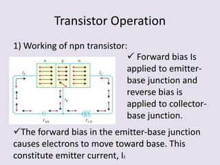
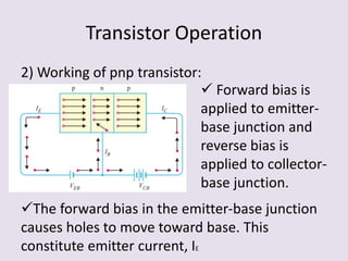
Downloaded 4,243 times


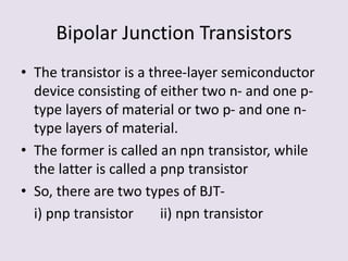
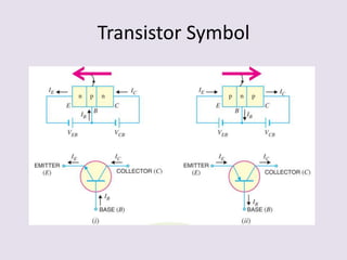
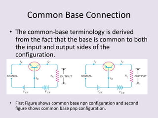


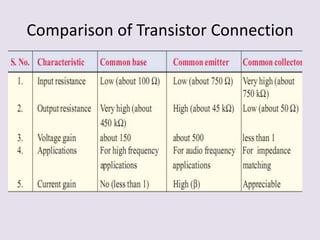
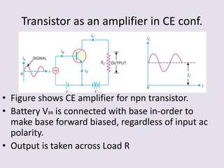


This presentation introduces bipolar junction transistors (BJTs). It discusses the two types of BJTs - NPN and PNP transistors, which differ based on whether holes or electrons are the majority carriers. The key components of a transistor - emitter, base, and collector - are defined. The presentation compares the three common transistor configurations - common base, common emitter, and common collector - and provides expressions for collector current in each. It also discusses transistor operation, characteristics, and applications such as amplification. Overall, the presentation provides a comprehensive overview of BJT fundamentals.


