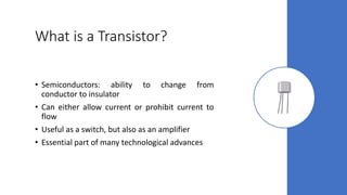
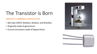
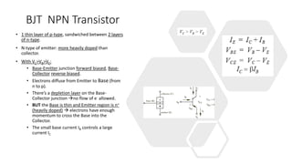
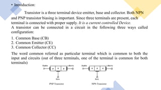
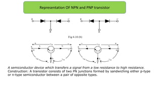
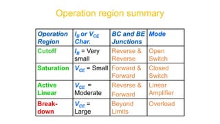
1. A transistor is a semiconductor device with three terminals (emitter, base, collector) that can amplify or switch electronic signals and electrical power. It was invented in 1947 as a replacement for vacuum tubes.
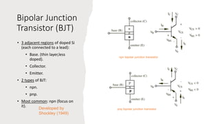
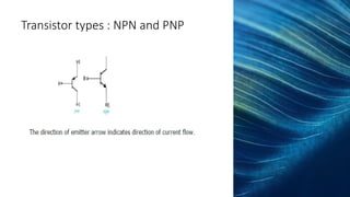
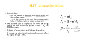
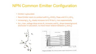
2. There are two main types of transistors - NPN and PNP. In an NPN transistor, the base-emitter junction is forward biased, allowing current to flow from the emitter to the collector. The small base current controls a much larger collector current.
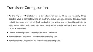
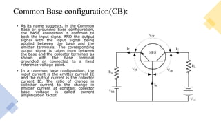
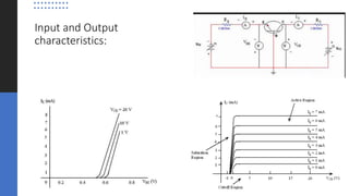
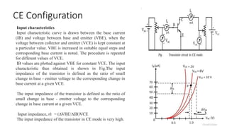
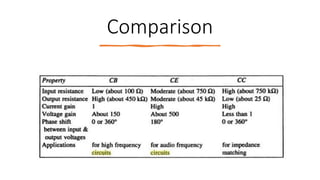
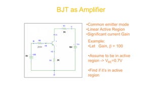
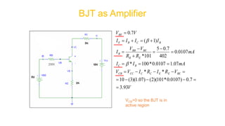
3. Transistors can be connected in common base, common emitter, or common collector configurations. The common emitter configuration provides both current and voltage gain and is widely used in amplifiers.
A Bipolar Junction Transistor is a three-terminal semiconductor device consisting of two p-n junctions which are able to amplify or magnify a signal. It is a current controlled device. The three terminals of the BJT are the base, the collector and the emitter. A BJT is a type of transistor that uses both electrons and holes as charge carriers
Transistors are the basic building blocks o almost all the electronic devices and circuits the hardware world is constantly dependent upon the transistor for its basic circuit and PCB designing and having a deep knowledge of transistor constructions, its types and working is essential for the development of Electronic circuits. This ppt is a basic and brief introduction to the construction and types of Transistors also addressed as BJT(Bipolar Junction Transistors) used for digital PCB and logic designing.
Water scarcity is the lack of fresh water resources to meet the standard water demand. There are two type of water scarcity. One is physical. The other is economic water scarcity.
TECHNICAL TRAINING MANUAL GENERAL FAMILIARIZATION COURSEDuvanRamosGarzon1
AIRCRAFT GENERAL
The Single Aisle is the most advanced family aircraft in service today, with fly-by-wire flight controls.
The A318, A319, A320 and A321 are twin-engine subsonic medium range aircraft.
The family offers a choice of engines
Welcome to WIPAC Monthly the magazine brought to you by the LinkedIn Group Water Industry Process Automation & Control.
In this month's edition, along with this month's industry news to celebrate the 13 years since the group was created we have articles including
A case study of the used of Advanced Process Control at the Wastewater Treatment works at Lleida in Spain
A look back on an article on smart wastewater networks in order to see how the industry has measured up in the interim around the adoption of Digital Transformation in the Water Industry.
Student information management system project report ii.pdfKamal Acharya
Our project explains about the student management. This project mainly explains the various actions related to student details. This project shows some ease in adding, editing and deleting the student details. It also provides a less time consuming process for viewing, adding, editing and deleting the marks of the students.
Quality defects in TMT Bars, Possible causes and Potential Solutions.PrashantGoswami42
Maintaining high-quality standards in the production of TMT bars is crucial for ensuring structural integrity in construction. Addressing common defects through careful monitoring, standardized processes, and advanced technology can significantly improve the quality of TMT bars. Continuous training and adherence to quality control measures will also play a pivotal role in minimizing these defects.
Saudi Arabia stands as a titan in the global energy landscape, renowned for its abundant oil and gas resources. It's the largest exporter of petroleum and holds some of the world's most significant reserves. Let's delve into the top 10 oil and gas projects shaping Saudi Arabia's energy future in 2024.
Sachpazis:Terzaghi Bearing Capacity Estimation in simple terms with Calculati...Dr.Costas Sachpazis
Terzaghi's soil bearing capacity theory, developed by Karl Terzaghi, is a fundamental principle in geotechnical engineering used to determine the bearing capacity of shallow foundations. This theory provides a method to calculate the ultimate bearing capacity of soil, which is the maximum load per unit area that the soil can support without undergoing shear failure. The Calculation HTML Code included.
Cosmetic shop management system project report.pdfKamal Acharya
Buying new cosmetic products is difficult. It can even be scary for those who have sensitive skin and are prone to skin trouble. The information needed to alleviate this problem is on the back of each product, but it's thought to interpret those ingredient lists unless you have a background in chemistry.
Instead of buying and hoping for the best, we can use data science to help us predict which products may be good fits for us. It includes various function programs to do the above mentioned tasks.
Data file handling has been effectively used in the program.
The automated cosmetic shop management system should deal with the automation of general workflow and administration process of the shop. The main processes of the system focus on customer's request where the system is able to search the most appropriate products and deliver it to the customers. It should help the employees to quickly identify the list of cosmetic product that have reached the minimum quantity and also keep a track of expired date for each cosmetic product. It should help the employees to find the rack number in which the product is placed.It is also Faster and more efficient way.
NO1 Uk best vashikaran specialist in delhi vashikaran baba near me online vas...Amil Baba Dawood bangali
Contact with Dawood Bhai Just call on +92322-6382012 and we'll help you. We'll solve all your problems within 12 to 24 hours and with 101% guarantee and with astrology systematic. If you want to take any personal or professional advice then also you can call us on +92322-6382012 , ONLINE LOVE PROBLEM & Other all types of Daily Life Problem's.Then CALL or WHATSAPP us on +92322-6382012 and Get all these problems solutions here by Amil Baba DAWOOD BANGALI
#vashikaranspecialist #astrologer #palmistry #amliyaat #taweez #manpasandshadi #horoscope #spiritual #lovelife #lovespell #marriagespell#aamilbabainpakistan #amilbabainkarachi #powerfullblackmagicspell #kalajadumantarspecialist #realamilbaba #AmilbabainPakistan #astrologerincanada #astrologerindubai #lovespellsmaster #kalajaduspecialist #lovespellsthatwork #aamilbabainlahore#blackmagicformarriage #aamilbaba #kalajadu #kalailam #taweez #wazifaexpert #jadumantar #vashikaranspecialist #astrologer #palmistry #amliyaat #taweez #manpasandshadi #horoscope #spiritual #lovelife #lovespell #marriagespell#aamilbabainpakistan #amilbabainkarachi #powerfullblackmagicspell #kalajadumantarspecialist #realamilbaba #AmilbabainPakistan #astrologerincanada #astrologerindubai #lovespellsmaster #kalajaduspecialist #lovespellsthatwork #aamilbabainlahore #blackmagicforlove #blackmagicformarriage #aamilbaba #kalajadu #kalailam #taweez #wazifaexpert #jadumantar #vashikaranspecialist #astrologer #palmistry #amliyaat #taweez #manpasandshadi #horoscope #spiritual #lovelife #lovespell #marriagespell#aamilbabainpakistan #amilbabainkarachi #powerfullblackmagicspell #kalajadumantarspecialist #realamilbaba #AmilbabainPakistan #astrologerincanada #astrologerindubai #lovespellsmaster #kalajaduspecialist #lovespellsthatwork #aamilbabainlahore #Amilbabainuk #amilbabainspain #amilbabaindubai #Amilbabainnorway #amilbabainkrachi #amilbabainlahore #amilbabaingujranwalan #amilbabainislamabad
Democratizing Fuzzing at Scale by Abhishek Aryaabh.arya
Presented at NUS: Fuzzing and Software Security Summer School 2024
This keynote talks about the democratization of fuzzing at scale, highlighting the collaboration between open source communities, academia, and industry to advance the field of fuzzing. It delves into the history of fuzzing, the development of scalable fuzzing platforms, and the empowerment of community-driven research. The talk will further discuss recent advancements leveraging AI/ML and offer insights into the future evolution of the fuzzing landscape.
3. What is a Transistor?
• Semiconductors: ability to change from
conductor to insulator
• Can either allow current or prohibit current to
flow
• Useful as a switch, but also as an amplifier
• Essential part of many technological advances
4. A Brief History
• Guglielmo Marconi invents radio in 1895
• Problem: For long distance travel, signal must be
amplified
• Lee De Forest improves on Fleming’s original
vacuum tube to amplify signals
• Made use of third electrode
• Too bulky for most applications
5. The Transistor is Born
• Bell Labs (1947): Bardeen, Brattain, and Shockley
• Originally made of germanium
• Current transistors made of doped silicon
6. How
Transistors
Work
Doping: adding small amounts of other
elements to create additional protons or
electrons
P-Type: dopants lack a fourth valence electron
(Boron, Aluminum)
N-Type: dopants have an additional (5th)
valence electron (Phosphorus, Arsenic)
Importance: Current only flows from P to N
7. Diodes and Bias
• Diode: simple P-N junction.
• Forward Bias: allows current to flow from P to N.
• Reverse Bias: no current allowed to flow from N to P.
• Breakdown Voltage: sufficient N to P voltage of a Zener
Diode will allow for current to flow in this direction.
8. Bipolar Junction
Transistor (BJT)
• 3 adjacent regions of doped Si
(each connected to a lead):
• Base. (thin layer,less
doped).
• Collector.
• Emitter.
• 2 types of BJT:
• npn.
• pnp.
• Most common: npn (focus on
it).
npn bipolar junction transistor
pnp bipolar junction transistor
Developed by
Shockley (1949)
9. BJT NPN Transistor
• 1 thin layer of p-type, sandwiched between 2 layers
of n-type.
• N-type of emitter: more heavily doped than
collector.
• With VC>VB>VE:
• Base-Emitter junction forward biased, Base-
Collector reverse biased.
• Electrons diffuse from Emitter to Base (from
n to p).
• There’s a depletion layer on the Base-
Collector junction →no flow of e- allowed.
• BUT the Base is thin and Emitter region is n+
(heavily doped) → electrons have enough
momentum to cross the Base into the
Collector.
• The small base current IB controls a large
current IC
10. • Introduction:
Transistor is a three terminal device emitter, base and collector. Both NPN
and PNP transistor biasing is important. Since three terminals are present, each
terminal is connected with proper supply. It is a current controlled Device.
A transistor can be connected in a circuit in the following three ways called
configuration:
1. Common Base (CB)
2. Common Emitter (CE)
3. Common Collector (CC)
The word common referred as particular terminal which is common to both the
input and circuits (out of three terminals, one of the terminal is common for both
terminals)
11. Representation OF NPN and PNP transistor
A semiconductor device which transfers a signal from a low resistance to high resistance.
Construction: A transistor consists of two PN junctions formed by sandwiching either p-type
or n-type semiconductor between a pair of opposite types.
13. Conventional Current Flow in npn: The base emitter junction is forward biased . allowing
low resistance in emitter (input) side & base-collector junction is reverse biased &
provides high resistance in collector(Output) side .
Accordingly the current flows from emitter towards base & collector
Therefore , Using Kirchhoff’s Current Law: IE = IB + IC
14. PNP transistor: Similarly, the in PNP , the current conduction is due to
majority carriers i.e. Holes as shown below. IE= IB + IC
15. Transistor Configuration
• As the Bipolar Transistor is a three-terminal device, there are basically three
possible ways to connect it within an electronic circuit with one terminal being common
to both the input and output. Each method of connection responding differently to its
input signal within a circuit as the static characteristics of the transistor vary with each
circuit arrangement.
• Common Base Configuration - has Voltage Gain but no Current Gain.
• Common Emitter Configuration - has both Current and Voltage Gain.
• Common Collector Configuration - has Current Gain but no Voltage Gain.
16. • Current Gain:
• α is the fraction of electrons that diffuse across the
narrow Base region
• 1- α is the fraction of electrons that recombine with
holes in the Base region to create base current
• The current Gain is expressed in terms of the β
(beta) of the transistor (often called hfe by
manufacturers).
• β (beta) is Temperature and Voltage dependent.
• It can vary a lot among transistors (common values
for signal BJT: 20 - 200).
BJT characteristics
−
=
=
−
=
=
1
)
1
(
B
C
E
B
E
C
I
I
I
I
I
I
17. Common Base configuration(CB):
• As its name suggests, in the Common
Base or grounded base configuration,
the BASE connection is common to
both the input signal AND the output
signal with the input signal being
applied between the base and the
emitter terminals. The corresponding
output signal is taken from between
the base and the collector terminals as
shown with the base terminal
grounded or connected to a fixed
reference voltage point.
• In a common base configuration, the
input current is the emitter current IE
and the output current is the collector
current IC. The ratio of change in
collector current to the change in
emitter current at constant collector
base voltage is called current
amplification factor.
•
20. • Emitter is grounded.
• Base-Emitter starts to conduct with VBE=0.6V,IC flows and it’s IC=*IB.
• Increasing IB, VBE slowly increases to 0.7V but IC rises exponentially.
• As IC rises ,voltage drop across RC increases and VCE drops toward ground.
(transistor in saturation, no more linear relation between IC and IB)
NPN Common Emitter Configuration
21. CE Configuration
Input characteristics
Input characteristic curve is drawn between the base current
(IB) and voltage between base and emitter (VBE), when the
voltage between collector and emitter (VCE) is kept constant at
a particular value. VBE is increased in suitable equal steps and
corresponding base current is noted. The procedure is repeated
for different values of VCE.
IB values are plotted against VBE for constant VCE. The input
characteristic thus obtained is shown in Fig.The input
impedance of the transistor is defined as the ratio of small
change in base - emitter voltage to the corresponding change in
base current at a given VCE.
The input impedance of the transistor is defined as the ratio of
small change in base - emitter voltage to the corresponding
change in base current at a given VCE.
Input impedance, r1 = (∆VBE/∆IB)VCE
The input impedance of the transistor in CE mode is very high.
22. Common Emitter characteristics
No current flows
Collector current
controlled by the
collector circuit.
(Switch behavior)
In full saturation
VCE=0.2V.
Collector current
proportional to
Base current
The avalanche
multiplication of
current through
collector junction
occurs: to be
avoided
23. Common
Collector
Configuration
• In common collector
configuration circuit is shown
in figure. Here collector is
grounded and it is used as the
common terminal for both
input and output. It is also
called as grounded collector
configuration. Base is used as a
input terminal whereas emitter
is the output terminal.
24. Input Characteristics
It is defined as the characteristic curve drawn between
input voltage to input current whereas output voltage is
constant.
To determine input characteristics, the emitter base
voltage VEB is kept constant at zero and base current IB
is increased from zero
by increasing VBC. This is repeated for higher fixed
values of VCE.A curve is drawn between base current and
base emitter voltage at constant collector base voltage
25. Output Characteristics
It is defined as the characteristic curve drawn between
output voltage to output current whereas input current is
constant.
To determine output characteristics, the base
current IB is kept constant at zero and emitter current IE
is increased from zero by increasing VEC.
This is repeated for higher fixed values of IB.
From the characteristic it is seen that for a constant value
of IB, IE is independent of VEB and the curves are
parallel to the axis of VEC.
27. Operation
Region
IB or VCE
Char.
BC and BE
Junctions
Mode
Cutoff IB = Very
small
Reverse &
Reverse
Open
Switch
Saturation VCE = Small Forward &
Forward
Closed
Switch
Active
Linear
VCE =
Moderate
Reverse &
Forward
Linear
Amplifier
Break-
down
VCE =
Large
Beyond
Limits
Overload
Operation region summary
28. BJT as Switch
•Vin(Low ) < 0.7 V
•BE junction not forward
biased
•Cutoff region
•No current flows
•Vout = VCE = Vcc
•Vout = High
•Vin(High)
•BE junction forward biased (VBE=0.7V)
•Saturation region
•VCE small (~0.2 V for saturated BJT)
•Vout = small
•IB = (Vin-VB)/RB
•Vout = Low
29. • Basis of digital logic circuits
• Input to transistor gate can be analog or digital
• Building blocks for TTL – Transistor Transistor Logic
• Guidelines for designing a transistor switch:
• VC>VB>VE
• VBE= 0.7 V
• IC independent from IB (in saturation).
• Min. IB estimated from by (IBmin IC/).
• Input resistance→ such that IB > 5-10 times IBmin because varies
among components, with temperature and voltage and RB may change
when current flows.
• Calculate the max IC and IB not to overcome device specifications.
BJT as Switch 2
30. •Common emitter mode
•Linear Active Region
•Significant current Gain
Example:
•Let Gain, = 100
•Assume to be in active
region -> VBE=0.7V
•Find if it’s in active
region
BJT as Amplifier