Downloaded 802 times


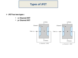
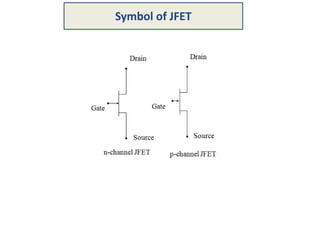


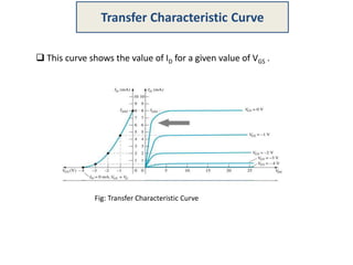


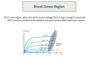


This document provides an overview of the Junction Field Effect Transistor (JFET). It discusses the construction of JFETs including the source, drain and gate terminals. It describes the theory of operation explaining how applying voltages to the gate can control the channel and current flow. The key sections outline the characteristic I-V curve, pinch-off voltage, saturation level and cut-off voltage. Advantages of JFETs are also summarized such as high input impedance. Common applications are listed including use as amplifiers and constant current sources.


